|
|
|
PDF EM6A8160TSA Data sheet ( Hoja de datos )
| Número de pieza | EM6A8160TSA | |
| Descripción | 4M x 16 DDR Synchronous DRAM | |
| Fabricantes | Etron Technology | |
| Logotipo | ||
Hay una vista previa y un enlace de descarga de EM6A8160TSA (archivo pdf) en la parte inferior de esta página. Total 30 Páginas | ||
|
No Preview Available !
EtronTech
EM6A8160TSA
Etron Confidential
4M x 16 DDR Synchronous DRAM (SDRAM)
Advanced (Rev. 1.2 Apr. /2009)
Features
• Fast clock rate: 200MHz
• Differential Clock CK & CK
• Bi-directional DQS
• DLL enable/disable by EMRS
• Fully synchronous operation
• Internal pipeline architecture
• Four internal banks, 1M x 16-bit for each bank
• Programmable Mode and Extended Mode Registers
- CAS Latency: 3
- Burst length: 2, 4, 8
- Burst Type: Sequential & Interleaved
• Individual byte writes mask control
• DM Write Latency = 0
• Auto Refresh and Self Refresh
• 4096 refresh cycles / 64ms
• Precharge & active power down
• Power supplies: VDD & VDDQ = 2.5V ± 5%
• Interface: SSTL_2 I/O Interface
• Package: 66 Pin TSOP II, 0.65mm pin pitch
- Pb free and Halogen free
Overview
The EM6A8160 SDRAM is a high-speed CMOS double
data rate synchronous DRAM containing 64 Mbits. It is
internally configured as a quad 1M x 16 DRAM with a
synchronous interface (all signals are registered on the
positive edge of the clock signal, CK). Data outputs occur at
both rising edges of CK and CK . Read and write accesses
to the SDRAM are burst oriented; accesses start at a
selected location and continue for a programmed number of
locations in a programmed sequence. Accesses begin with
the registration of a BankActivate command which is then
followed by a Read or Write command. The EM6A8160
provides programmable Read or Write burst lengths of 2, 4,
8. An auto precharge function may be enabled to provide a
self-timed row precharge that is initiated at the end of the
burst sequence. The refresh functions, either Auto or Self
Refresh are easy to use. In addition, EM6A8160 features
programmable DLL option. By having a programmable
mode register and extended mode register, the system can
choose the most suitable modes to maximize its
performance. These devices are well suited for applications
requiring high memory bandwidth and high performance.
Table 1.Ordering Information
Part Number
Clock
Frequency
Data Rate
Package
EM6A8160TSA-5G 200MHz 400Mbps/pin TSOPII
TS: indicates TSOP II package
A: indicates Generation Code
G: indicates Pb and Halogen Free for TSOPII Package
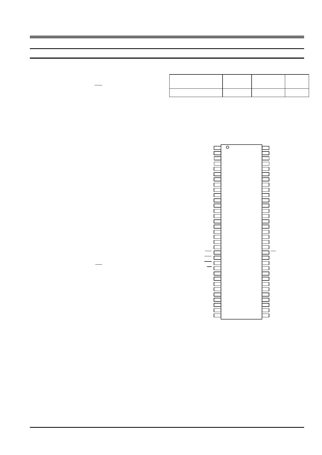
Figure 1. Pin Assignment (Top View)
VDD
DQ0
VDDQ
DQ1
DQ2
VSSQ
DQ3
DQ4
VDDQ
DQ5
DQ6
VSSQ
DQ7
NC
VDDQ
LDQS
NC
VDD
NC
LDM
WE
CAS
RAS
CS
NC
BA0
BA1
A10/AP
A0
A1
A2
A3
VDD
1
2
3
4
5
6
7
8
9
10
11
12
13
14
15
16
17
18
19
20
21
22
23
24
25
26
27
28
29
30
31
32
33
66 VSS
65 DQ15
64 VSSQ
63 DQ14
62 DQ13
61 VDDQ
60 DQ12
59 DQ11
58 VSSQ
57 DQ10
56 DQ9
55 VDDQ
54 DQ8
53 NC
52 VSSQ
51 UDQS
50 NC
49 VREF
48 VSS
47 UDM
46 CK
45 CK
44 CKE
43 NC
42 NC
41 A11
40 A9
39 A8
38 A7
37 A6
36 A5
35 A4
34 VSS
Etron Technology, Inc.
No. 6, Technology Rd. V, Hsinchu Science Park, Hsinchu, Taiwan 30078, R.O.C.
TEL: (886)-3-5782345 FAX: (886)-3-5778671
Etron Technology, Inc. reserves the right to change products or specification without notice.
1 page 
EtronTech
EM6A8160TSA
Operation Mode
Fully synchronous operations are performed to latch the commands at the positive edges of CK. Table 3
shows the truth table for the operation commands.
Table 3. Truth Table (Note (1), (2))
Command
State CKEn-1 CKEn UDM LDM BA0,1 A10 A0-9,11 CS RAS CAS WE
BankActivate
Idle(3)
H X X X V Row address L L H H
BankPrecharge
Any H X X X V L X L L H L
PrechargeAll
Any H X X X X H X L L H L
Write
Write and AutoPrecharge
Active(3) H X X X V L Column L H L L
address
Active(3) H X X X V H (A0 ~ A7) L H L L
Read
Read and Autoprecharge
Active(3) H X X X V L Column L H L H
address
Active(3) H X X X V H (A0 ~ A7) L H L H
Mode Register Set
Idle H X X X
OP code
LL L L
Extended MRS
Idle H X X X
OP code
LL L L
No-Operation
Any H X X X X X X L H H H
Burst Stop
Active(4) H X X X X X X L H H L
Device Deselect
Any H X X X X X X H X X X
AutoRefresh
Idle H H X X X X X L L L H
SelfRefresh Entry
Idle H L X X X X X L L L H
SelfRefresh Exit
Idle L H X X X X X H X X X
(SelfRefresh)
LH H H
Precharge Power Down Mode
Entry
Idle
H L X X X X X HX X X
LH H H
Precharge Power Down Mode
Any
Exit
(PowerDown)
L
H X X X X X HX X X
LH H H
Active Power Down Mode
Entry
Active
H L X X X X X HX X X
LV V V
Active Power Down Mode
Exit
Any
(PowerDown)
L
H X X X X X HX X X
LH H H
Data Input Mask Disable
Active
H X L L X X X XX X X
Data Input Mask Enable(5)
Active
H X H H X X X XX X X
Note: 1. V=Valid data, X=Don't Care, L=Low level, H=High level
2. CKEn signal is input level when commands are provided.
CKEn-1 signal is input level one clock cycle before the commands are provided.
3. These are states of bank designated by BA signal.
4. Device state is 2, 4, 8, burst operation.
5. LDM and UDM can be enabled respectively.
Etron Confidential
5
Rev 1.2
Apr. 2009
5 Page 
EtronTech
EM6A8160TSA
Table 15. D.C. Characteristics (VDD = 2.5V ± 5%, TA = 0~70 °C)
Parameter & Test Condition
Symbol
OPERATING CURRENT : One bank; Active-Precharge; tRC=tRC(min);
tCK=tCK(min); DQ,DM and DQS inputs changing once per clock cycle;
Address and control inputs changing once every two clock cycles.
OPERATING CURRENT : One bank; Active-Read-Precharge; BL=4;
tRC=tRC(min); tCK=tCK(min); lout=0mA; Address and control inputs
changing once per clock cycle
PRECHARGE POWER-DOWN STANDBY CURRENT: All banks idle;
power-down mode; tCK=tCK(min); CKE=LOW
IDD0
IDD1
IDD2P
-5
Max
120
140
10
Unit
mA
mA
mA
IDLE STANDLY CURRENT : CKE = HIGH; CS =HIGH(DESELECT); All
banks idle; tCK=tCK(min); Address and control inputs changing once per IDD2N 50 mA
clock cycle; VIN=VREF for DQ, DQS and DM
ACTIVE POWER-DOWN STANDBY CURRENT : one bank active;
power-down mode; CKE=LOW; tCK=tCK(min)
IDD3P
40 mA
ACTIVE STANDBY CURRENT : CS =HIGH;CKE=HIGH; one bank
active ; tRC=tRC(max);tCK=tCK(min);Address and control inputs changing IDD3N 80 mA
once per clock cycle; DQ,DQS,and DM inputs changing twice per clock
cycle
OPERATING CURRENT BURST READ : BL=2; READs; Continuous
burst; one bank active; Address and control inputs changing once per
clock cycle; tCK=tCK(min); lout=0mA;50% of data changing on every
IDD4R
180
mA
transfer
OPERATING CURRENT BURST Write : BL=2; WRITEs; Continuous
Burst ;one bank active; address and control inputs changing once per
clock cycle; tCK=tCK(min); DQ,DQS,and DM changing twice per clock
IDD4W
180
mA
cycle; 50% of data changing on every transfer
AUTO REFRESH CURRENT : tRC=tRFC(min); tCK=tCK(min)
IDD5
180 mA
SELF REFRESH CURRENT: Self Refresh Mode ; CKE
0.2V;tCK=tCK(min)
BURST OPERATING CURRENT 4 bank operation:
Four bank interleaving READs; BL=4;with Auto Precharge;
tRC=tRC(min); tCK=tCK(min); Address and control inputs change only
during Active, READ , or WRITE command
IDD6
IDD7
4 mA
240 mA
Figure 3. Timing Waveform for IDD7 Measurement at 200 MHz CK Operation
CK
CK
tRCD
COMMAND ACT
ADDRESS
Bank 0
Row d
READ
AP
ACT
READ
AP
ACT
READ
AP
ACT
READ
AP
ACT
Bank 3
Col c
Bank 1
Row e
Bank 0
Col d
Bank 2
Row f
CL=3
Bank 1
Col e
Bank 3
Row g
Bank 2
Col f
Bank 0
Row h
...pattern repeats...
DQS
DQ D0 a D0 a D0 a D0 a D0 b D0 b D0 b D0 b D0 c D0 c D0 c D0 c D0 d D0 d D0 d D0 d D0 e D0 e D0 e D0 e D0 f D0 f
Etron Confidential
11 Rev 1.2 Apr. 2009
11 Page | ||
| Páginas | Total 30 Páginas | |
| PDF Descargar | [ Datasheet EM6A8160TSA.PDF ] | |
Hoja de datos destacado
| Número de pieza | Descripción | Fabricantes |
| EM6A8160TSA | 4M x 16 DDR Synchronous DRAM | Etron Technology |
| Número de pieza | Descripción | Fabricantes |
| SLA6805M | High Voltage 3 phase Motor Driver IC. |
Sanken |
| SDC1742 | 12- and 14-Bit Hybrid Synchro / Resolver-to-Digital Converters. |
Analog Devices |
|
DataSheet.es es una pagina web que funciona como un repositorio de manuales o hoja de datos de muchos de los productos más populares, |
| DataSheet.es | 2020 | Privacy Policy | Contacto | Buscar |