|
|
|
PDF ADG1402 Data sheet ( Hoja de datos )
| Número de pieza | ADG1402 | |
| Descripción | SPST Switches | |
| Fabricantes | Analog Devices | |
| Logotipo | ||
Hay una vista previa y un enlace de descarga de ADG1402 (archivo pdf) en la parte inferior de esta página. Total 16 Páginas | ||
|
No Preview Available !
1 Ω On Resistance, ±15 V/+12 V/±5 V
iCMOS SPST Switches
ADG1401/ADG1402
FEATURES
1 Ω on resistance
0.2 Ω on resistance flatness
Up to 430 mA continuous current
Fully specified at +12 V, ±15 V, ±5 V
No VL supply required
3 V logic-compatible inputs
Rail-to-rail operation
8-lead MSOP and 8-lead, 3 mm × 2 mm LFCSP packages
APPLICATIONS
Automatic test equipment
Data acquisition systems
Battery-powered systems
Sample-and-hold systems
Audio signal routing
Video signal routing
Communication systems
Relay replacements
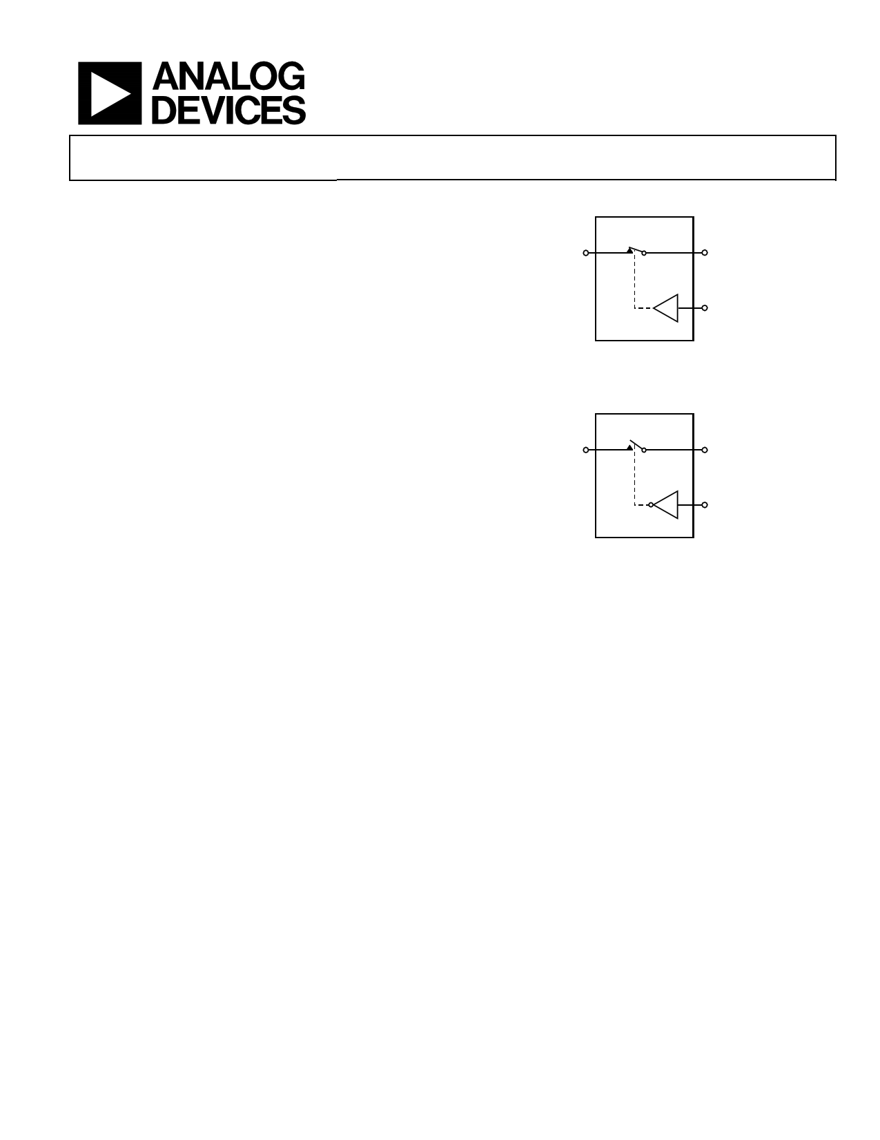
FUNCTIONAL BLOCK DIAGRAM
ADG1401
SD
IN
SWITCHES SHOWN FOR A LOGIC 1 INPUT
Figure 1. ADG1401 Functional Block Diagram
ADG1402
SD
IN
SWITCHES SHOWN FOR A LOGIC 1 INPUT
Figure 2. ADG1402 Functional Block Diagram
GENERAL DESCRIPTION
The ADG1401/ADG1402 contain a single-pole/single-throw
(SPST) switch. Figure 1 shows that with a logic input of 1, the
switch of the ADG1401 is closed and that of the ADG1402 is
open. Each switch conducts equally well in both directions when
on and has an input signal range that extends to the supplies. In
the off condition, signal levels up to the supplies are blocked.
The iCMOS® (industrial CMOS) modular manufacturing process
combines high voltage, complementary metal-oxide semiconductor
(CMOS) and bipolar technologies. It enables the development
of a wide range of high performance analog ICs capable of 33 V
operation in a footprint that no other generation of high voltage
parts has achieved. Unlike analog ICs using conventional CMOS
processes, iCMOS components can tolerate high supply voltages
while providing increased performance, dramatically lower
power consumption, and a reduced package size.
The on resistance profile is very flat over the full analog input
range ensuring excellent linearity and low distortion when
switching audio signals. The iCMOS construction ensures
ultralow power dissipation, making the part ideally suited for
portable and battery-powered instruments.
PRODUCT HIGHLIGHTS
1. 1.3 Ω maximum on resistance at 25°C.
2. Minimum distortion.
3. 3 V logic-compatible digital inputs: VINH = 2.0 V, VINL = 0.8 V.
4. No VL logic power supply required.
5. 8-lead MSOP and 8-lead, 3 mm × 2 mm LFCSP packages.
Rev. 0
Information furnished by Analog Devices is believed to be accurate and reliable. However, no
responsibility is assumed by Analog Devices for its use, nor for any infringements of patents or other
rights of third parties that may result from its use. Specifications subject to change without notice. No
license is granted by implication or otherwise under any patent or patent rights of Analog Devices.
Trademarksandregisteredtrademarksarethepropertyoftheirrespectiveowners.
One Technology Way, P.O. Box 9106, Norwood, MA 02062-9106, U.S.A.
Tel: 781.329.4700
www.analog.com
Fax: 781.461.3113
©2009 Analog Devices, Inc. All rights reserved.
1 page 
ADG1401/ADG1402
±5 V DUAL SUPPLY
VDD = +5 V ± 10%, VSS = −5 V ± 10%, GND = 0 V, unless otherwise noted.
Table 3.
Parameter
ANALOG SWITCH
Analog Signal Range
On Resistance, RON
On Resistance Flatness, RFLAT (ON)
LEAKAGE CURRENTS
Source Off Leakage, IS (Off )
Drain Off Leakage, ID (Off )
Channel On Leakage, ID, IS (On)
DIGITAL INPUTS
Input High Voltage, VINH
Input Low Voltage, VINL
Input Current, IINL or IINH
Digital Input Capacitance, CIN
DYNAMIC CHARACTERISTICS1
tON
tOFF
Charge Injection
Off Isolation
Total Harmonic Distortion + Noise
−40°C to −40°C to
25°C +85°C
+125°C
2.3
2.7 3.3
0.65
0.72 0.85
0 V to VDD
3.7
0.9
±0.02
±0.4
±0.02
±0.4
±0.1
±1
±3
±3
±3
±150
±150
±150
0.002
4
2.0
0.8
±0.1
290
375 460
235
305 365
145
−58
0.02
520
405
−3 dB Bandwidth
Insertion Loss
CS (Off )
CD (Off )
CD, CS (On)
POWER REQUIREMENTS
IDD
79
0.14
52
58
198
0.001
ISS 0.001
VDD/VSS
1 Guaranteed by design, not subject to production test.
1.0
1.0
±4.5/±16.5
Unit
V
Ω typ
Ω max
Ω typ
Ω max
nA typ
nA max
nA typ
nA max
nA typ
nA max
V min
V max
μA typ
μA max
pF typ
ns typ
ns max
ns typ
ns max
pC typ
dB typ
% typ
MHz typ
dB typ
pF typ
pF typ
pF typ
μA typ
μA max
μA typ
μA max
V min/max
Test Conditions/Comments
VS = ±4.5 V, IS = −10 mA; see Figure 20
VDD = +4.5 V, VSS = −4.5 V
VS = ±4.5 V, IS = −10 mA
VDD = +5.5 V, VSS = −5.5 V
VS = ±4.5 V, VD = ∓4.5 V; see Figure 21
VS = ±4.5 V, VD = ∓4.5 V; see Figure 21
VS = VD = ±4.5 V; see Figure 22
VIN = VGND or VDD
RL = 300 Ω, CL = 35 pF
VS = 3 V; see Figure 23
RL = 300 Ω, CL = 35 pF
VS = 3 V; see Figure 23
VS = 0 V, RS = 0 Ω, CL = 1 nF; see Figure 24
RL = 50 Ω, CL = 5 pF, f = 1 MHz; see Figure 25
RL = 10 kΩ, 5 V p-p, f = 20 Hz to 20 kHz;
see Figure 27
RL = 50 Ω, CL = 5 pF; see Figure 26
RL = 50 Ω, CL = 5 pF, f = 1 MHz; see Figure 26
VS = 0 V, f = 1 MHz
VS = 0 V, f = 1 MHz
VS = 0 V, f = 1 MHz
VDD = +5.5 V, VSS = −5.5 V
Digital inputs = 0 V or VDD
Digital inputs = 0 V or VDD
Ground = 0 V
Rev. 0 | Page 5 of 16
5 Page 
0
TA = 25°C
VDD = +15V
VSS = –15V
–20
–40
–60
–80
–100
–120
1k
10k 100k 1M 10M 100M
FREQUENCY (Hz)
Figure 16. Off Isolation vs. Frequency
1G
0
–0.5
–1.0
–1.5
–2.0
–2.5
–3.0
–3.5
–4.0
10k
TA = 25°C
VDD = +15V
VSS = –15V
100k 1M 10M 100M
FREQUENCY (Hz)
Figure 17. On Response vs. Frequency
1G
ADG1401/ADG1402
0.030
RL = 110Ω
TA = 25°C
0.025
VDD = 5V, VSS = 5V, VS = 5V p-p
0.020
0.015
0.010
0.005
VDD = 15V, VSS = 15V, VS = 10V p-p
0
0 5k 10k 15k
FREQUENCY (Hz)
Figure 18. THD + N vs. Frequency
0
TA = 25°C
–10 VDD = +15V
VSS = –15V
–20
–30
–40
–50
–60
–70
–80
–90
–100
1k
10k
NO DECOUPLING
CAPACITORS
DECOUPLING
CAPACITORS
100k
FREQUENCY (Hz)
1M
Figure 19. ACPSRR vs. Frequency
20k
10M
Rev. 0 | Page 11 of 16
11 Page | ||
| Páginas | Total 16 Páginas | |
| PDF Descargar | [ Datasheet ADG1402.PDF ] | |
Hoja de datos destacado
| Número de pieza | Descripción | Fabricantes |
| ADG1401 | SPST Switches | Analog Devices |
| ADG1402 | SPST Switches | Analog Devices |
| ADG1404 | Multiplexer | Analog Devices |
| ADG1406 | CMOS Multiplexers | Analog Devices |
| Número de pieza | Descripción | Fabricantes |
| SLA6805M | High Voltage 3 phase Motor Driver IC. |
Sanken |
| SDC1742 | 12- and 14-Bit Hybrid Synchro / Resolver-to-Digital Converters. |
Analog Devices |
|
DataSheet.es es una pagina web que funciona como un repositorio de manuales o hoja de datos de muchos de los productos más populares, |
| DataSheet.es | 2020 | Privacy Policy | Contacto | Buscar |