|
|
|
PDF 8SLVD2102 Data sheet ( Hoja de datos )
| Número de pieza | 8SLVD2102 | |
| Descripción | LVDS Output Fanout Buffer | |
| Fabricantes | IDT | |
| Logotipo | ||
Hay una vista previa y un enlace de descarga de 8SLVD2102 (archivo pdf) en la parte inferior de esta página. Total 18 Páginas | ||
|
No Preview Available !
Dual 1:2, LVDS Output Fanout Buffer
8SLVD2102
DATA SHEET
General Description
The 8SLVD2102 is a high-performance differential dual 1:2 LVDS
fanout buffer. The device is designed for the fanout of high-frequency,
very low additive phase-noise clock and data signals. The
8SLVD2102 is characterized to operate from a 2.5V power supply.
Guaranteed output-to-output and part-to-part skew characteristics
make the 8SLVD2102 ideal for those clock distribution applications
demanding well-defined performance and repeatability. Two
independent buffers with two low skew outputs each are available.
The integrated bias voltage generators enables easy interfacing of
single-ended signals to the device inputs. The device is optimized for
low power consumption and low additive phase noise.
Features
• Two 1:2, low skew, low additive jitter LVDS fanout buffers
• Two differential clock inputs
• Differential pairs can accept the following differential input
levels: LVDS and LVPECL
• Maximum input clock frequency: 2GHz
• Output bank skew: 15ps (maximum)
• Propagation delay: 300ps (maximum)
• Low additive phase jitter: 200fs, RMS (maximum);
fREF = 156.25MHz, VPP = 1V, VCMR = 1V,
Integration Range 10kHz - 20MHz
• 2.5V supply voltage
• Maximum device current consumption (IDD): 90mA
• Lead-free (RoHS 6) 16-Lead VFQFN package
• -40°C to 85°C ambient operating temperature
Block Diagram
VDD
PCLKA
nPCLKA
PCLKB
nPCLKB
VDD
VREF
EN
Voltage
VDD Reference
QA0
nQA0
QA1
nQA1
QB0
nQB0
QB1
nQB1
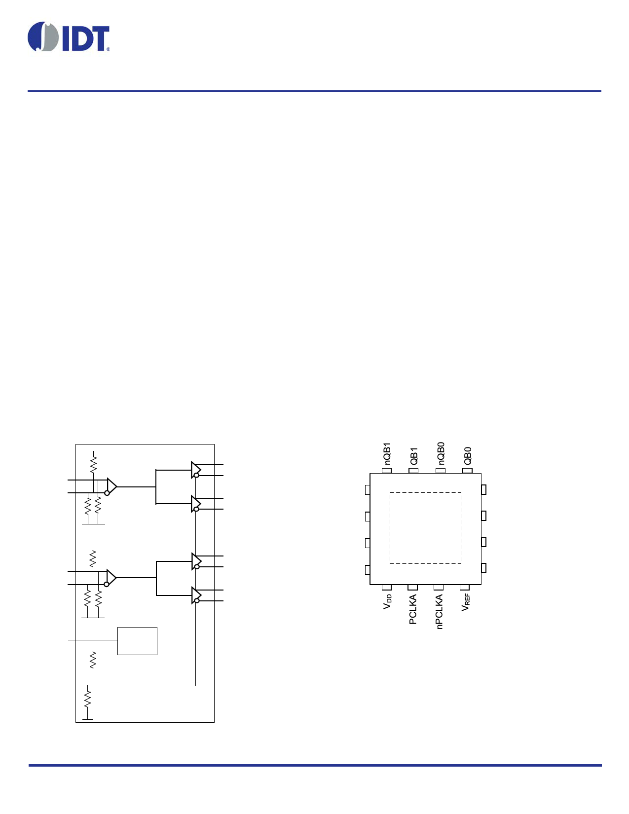
Pin Assignment
16 15 14 13
GND 1
12 nQA1
EN 2
PCLKB 3
8SLVD2102I
8XXXXXX
11 QA1
10 nQA0
nPCLKB 4
9 QA0
56 7 8
16-pin, 3.0mm x 3.0mm VFQFN Package
8SLVD2102 REVISION 2 11/11/15 1 ©2015 Integrated Device Technology, Inc.
1 page 
8SLVD2102 DATA SHEET
Table 5. AC Electrical Characteristics, VDD = 2.5V ± 5%, TA = -40°C to 85°C
Symbol Parameter
Test Conditions
Minimum
Typical
Maximum
Units
fREF
V/t
Input Frequency
Input Edge Rate
2 GHz
0.75 V/ns
PCLKA, nPCLKA to QA[0:1], nQA[0:1],
tPD Propagation Delay; NOTE 1 PCLKB, nPCLKB to QB[0:1], nQB[0:1]
100
196
300
ps
Channel Isolation
75 dB
tsk(o) Output Skew; NOTE 2, 3
QA[0:1], nQA[0:1], QB[0:1], nQB[0:1]
14 40 ps
tsk(b) Output Bank Skew; NOTE 3
Between Outputs within Each Bank
7 15 ps
tsk(p)
tsk(pp)
Pulse Skew
Part-to-Part Skew; NOTE 3, 4
50% Input Duty Cycle, fREF = 100MHz
-50
50 ps
200 ps
fREF = 1228.8MHz, VPP = 0.2V, VCMR = 1V
Integration Range: 10kHz – 20MHz
tJIT
Buffer Additive Phase Jitter,
RMS; refer to Additive Phase
Jitter Section
fREF = 156.25MHz, VPP = 0.5V, VCMR = 1V
Integration Range: 10kHz – 20MHz
fREF = 156.25MHz, VPP = 1V, VCMR = 1V
Integration Range: 10kHz – 20MHz
20 50 fs
140 250 fs
80 200 fs
tJIT, SP
Spurious Suppression,
Coupling from QA1 to QB0
tR / tF Output Rise/ Fall Time
fQB0 = 500MHz, VPP (PCLKB) = 0.15V,
VCMR(PCLKB) = 1V and
fQA1 = 62.5MHz, VPP(PCLKA) = 1V,
VCMR(PCLKA) = 1V
fQB0 = 500MHz, VPP (PCLKB) = 0.15V,
VCMR(PCLKB) = 1V and
fQA1 = 15.625MHz, VPP (PCLKA) = 1V,
VCMR(PCLKA) = 1V
20% to 80%
68 dB
74 dB
120 200 ps
NOTE: Electrical parameters are guaranteed over the specified ambient operating temperature range, which is established when the device is
mounted in a test socket with maintained transverse airflow greater than 500 lfpm. The device will meet specifications after thermal equilibrium
has been reached under these conditions.
NOTE 1: Measured from the differential input crossing point to the differential output crossing point.
NOTE 2: Defined as skew between outputs at the same supply voltage and with equal load conditions.
Measured at the differential cross points.
NOTE 3: This parameter is defined in accordance with JEDEC Standard 65.
NOTE 4: Defined as skew between outputs on different devices operating at the same supply voltages and with equal load conditions. Using
the same type of inputs on each device, the outputs are measured at the differential cross points.
REVISION 2 11/11/15
5 DUAL 1:2, LVDS OUTPUT FANOUT BUFFER
5 Page 
8SLVD2102 DATA SHEET
LVDS Driver Termination
For a general LVDS interface, the recommended value for the
termination impedance (ZT) is between 90 and 132. The actual
value should be selected to match the differential impedance (Z0) of
your transmission line. A typical point-to-point LVDS design uses a
100 parallel resistor at the receiver and a 100 differential
transmission-line environment. In order to avoid any
transmission-line reflection issues, the components should be
surface mounted and must be placed as close to the receiver as
possible. IDT offers a full line of LVDS compliant devices with two
types of output structures: current source and voltage source. The
standard termination schematic as shown in Figure 3A can be used
with either type of output structure. Figure 3B, which can also be
used with both output types, is an optional termination with center tap
capacitance to help filter common mode noise. The capacitor value
should be approximately 50pF. If using a non-standard termination, it
is recommended to contact IDT and confirm if the output structure is
current source or voltage source type. In addition, since these
outputs are LVDS compatible, the input receiver’s amplitude and
common-mode input range should be verified for compatibility with
the output.
LVDS
Driver
ZO ZT
Figure 3A. Standard Termination
LVDS
ZT Receiver
LVDS
Driver
ZO ZT
Figure 3B. Optional Termination
LVDS Termination
ZT
2 LVDS
C ZT Receiver
2
REVISION 2 11/11/15
11 DUAL 1:2, LVDS OUTPUT FANOUT BUFFER
11 Page | ||
| Páginas | Total 18 Páginas | |
| PDF Descargar | [ Datasheet 8SLVD2102.PDF ] | |
Hoja de datos destacado
| Número de pieza | Descripción | Fabricantes |
| 8SLVD2102 | LVDS Output Fanout Buffer | IDT |
| 8SLVD2104 | LVDS Output Fanout Buffer | IDT |
| Número de pieza | Descripción | Fabricantes |
| SLA6805M | High Voltage 3 phase Motor Driver IC. |
Sanken |
| SDC1742 | 12- and 14-Bit Hybrid Synchro / Resolver-to-Digital Converters. |
Analog Devices |
|
DataSheet.es es una pagina web que funciona como un repositorio de manuales o hoja de datos de muchos de los productos más populares, |
| DataSheet.es | 2020 | Privacy Policy | Contacto | Buscar |