|
|
|
PDF A4450 Data sheet ( Hoja de datos )
| Número de pieza | A4450 | |
| Descripción | Buck-Boost Controller | |
| Fabricantes | Allegro | |
| Logotipo | ||
Hay una vista previa y un enlace de descarga de A4450 (archivo pdf) en la parte inferior de esta página. Total 30 Páginas | ||
|
No Preview Available !
A4450
Buck-Boost Controller with Integrated Buck MOSFET
FEATURES AND BENEFITS
• Automotive AEC-Q100 qualified
• Wide operating range of 3 to 36 VIN, 40 VIN maximum,
covers automotive stop/start, cold crank, double battery,
and load dump
• Regulated output can range from 3 to 8 V at up to 1 A DC
• Adjustable PWM switching frequency:
250 kHz to 2.2 MHz
• PWM frequency can be synchronized to external clock:
250 kHz to 2.4 MHz
• Frequency dithering helps reduce EMI/EMC
• Undervoltage protection
• Pin-to-pin and pin-to-ground tolerant at every pin
• Thermal shutdown protection
• Operating junction temperature range −40°C to 150°C
PACKAGES:
20-pin 4 × 4 mm QFN (ES) with wettable flank
Not to scale
DESCRIPTION
The A4450 is a power management IC that can implement
either a buck or buck-boost regulator to efficiently convert
automotive battery voltages into a tightly regulated voltage. It
includes control, diagnostics, and protection functions.
An enable input to the A4450 is compatible to a high-voltage
battery level, (EN).
A diagnostic output from the A4450 includes a power-on reset
output (NPOR) signal.
Protection features include pulse-by-pulse current limit, hiccup
mode short-circuit protection, LX short-circuit protection,
missing freewheeling diode (buck diode at LX node in A4450)
protection, and thermal shutdown.
The A4450 is most suitable for applications where the input
voltage can vary from less than or greater than the regulated
output voltage.
The A4450 is supplied in 4 × 4 mm QFN (suffix “ES”) with
exposed power pad.
APPLICATIONS
• Infotainment
• Instrument Clusters
• Control Modules
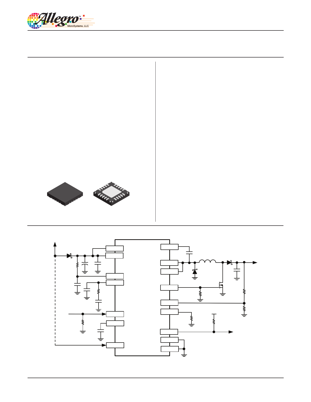
VBAT
VIN
A4450-DS
VIN
VIN
AVIN
COMP
A4450
FSET /SYNC
SS
EN
BOOT
LX
LX
LG
FB
RNG
NPOR
GND
PGND
D1
Buck
Diode
Typical Application Diagram
D2 Boost
Diode
VOUT
1 page 
A4450
Buck-Boost Controller
with Integrated Buck MOSFET
ELECTRICAL CHARACTERISTICS: Valid at 3 V ≤ VIN ≤ 36 V and VIN having first reached VINSTART,
‒40°C ≤ TJ ≤ 150°C, unless noted otherwise
Characteristics
Symbol
Test Conditions
Min. Typ.
GENERAL SPECIFICATIONS
Operating Input Voltage
VIN
VIN UVLO Start
VINSTART
VIN UVLO Stop
VINSTOP
Supply Quiescent Current 1
IQ
IQ(SLEEP)
PWM SWITCHING FREQUENCY AND DITHERING
After VIN > VINSTART, VEN ≥ 4 V
VIN rising
VIN falling, when in Buck-Boost mode
VIN = 13.5 V, VEN ≥ 4 V, no load
VIN = 13.5 V, VEN ≤ 1 V, no load
3.0 13.5
––
––
– 4.5
––
Switching Frequency
Frequency Dithering
VIN Dithering START Threshold
VIN Dithering STOP Threshold
VIN Dithering Hysteresis
THERMAL PROTECTION
fOSC
ΔfOSC
VIN(DITHER,ON)
VIN(DITHER,OFF)
VIN(DITHER,HYS)
RFSET = 7.87 kΩ
RFSET = 41.2 kΩ
As a percent of fOSC
VIN rising, RNG = 15 kΩ, target VOUT = 5 V
VIN falling
VIN falling, RNG = 15 kΩ, target VOUT = 5 V
VIN rising
1.8 2.0
343 400
– ±12
7.0*
– 16.6
7.0*
– 18
– 1.5
Thermal Shutdown Threshold 2
Thermal Shutdown Hysteresis 2
OUTPUT VOLTAGE SPECIFICATIONS
TTSD
THYS
TJ rising
160 170
– 20
Feedback Voltage Tolerance
PULSE-WIDTH MODULATION (PWM)
VFB
VIN = 13.5 V, EN = high
0.788 0.800
PWM Ramp Offset
LX Rising Slew Rate 2
LX Falling Slew Rate 2
Buck Minimum On-Time
Buck Minimum Off-Time
Boost Maximum Duty Cycle
COMP to LX Current Gain
Slope Compensation 2
INTERNAL MOSFET
VPWMOFFS
LXRISE
LXFALL
tON(MIN,BUCK)
tOFF(MIN,BUCK)
DMAX(BST)
gmPOWER
SE
VCOMP for 0% duty cycle
VIN = 13.5 V, 10% to 90%, ILX = 1 A
VIN = 13.5 V, 10% to 90%, ILX = 1 A
VIN = 3.5 V, VOUT = 8 V target, RNG = 25.5 kΩ, 2 MHz
VIN = 3.5 V, VOUT = 5 V target, RNG = 15 kΩ, 2 MHz
VIN = 3.5 V, VOUT = 3 V target, RNG = 9.31 kΩ, 2 MHz
fOSC = 2 MHz
fOSC = 400 kHz
–
–
–
–
–
–
–
–
3.5
1.76
0.35
400
1.5
1.8
85
85
0.75
0.57
0.31
4.7
2.2
0.44
MOSFET On Resistance
MOSFET Leakage
RDSon
IFET(LKG)
VIN = 13.5 V, TJ = –40°C (2), IDS = 0.1 A
VIN = 13.5 V, TJ = 25°C (2), IDS = 0.1 A
VIN = 13.5 V, TJ = 150°C, IDS = 0.1 A
VEN ≤ 1 V, VLX = 0 V, VIN = 13.5 V,
−40°C ≤ TJ ≤ 85°C (2)
– 60
– 80
– 140
––
Continued on the next page…
Max.
36
4.8
2.9
–
10
2.2
457
–
–
–
–
180
–
0.812
–
–
–
120
120
–
–
–
5.9
2.64
0.53
90
110
170
10
Unit
V
V
V
mA
µA
MHz
kHz
%
V
V
V
V
V
°C
°C
V
mV
V/ns
V/ns
ns
ns
–
–
–
A/V
A/µs
A/µs
mΩ
mΩ
mΩ
µA
Allegro MicroSystems, LLC
115 Northeast Cutoff
Worcester, Massachusetts 01615-0036 U.S.A.
1.508.853.5000; www.allegromicro.com
5
5 Page 
A4450
Buck-Boost Controller
with Integrated Buck MOSFET
Under the Buck-Boost mode operation, the buck switch duty
cycle, DBuck, is controlled through the feedback network to regu-
late VOUT, as shown in the equation below:
VOUT = DBuck / (1 – DBoost) × VIN (4)
This dual mode controller of A4450 enables smooth transition
between Buck and Buck-Boost mode over a wide range of input
voltages to maintain the regulation of output voltages.
Take as an example, VOUT = 5 V buck-boost regulator, setting
DBUCK0 = 0.61 results in RNG = 15 kΩ from equation 4. As
shown in Figure 2, when VIN is greater than ~8.5 V, the regulator
is in Buck mode and the duty cycle of Boost switch is 0; when
VIN is less than ~8.5 V, the regulator enters is in Buck-Boost
mode with both switches turning on and off. It is recommended
that the duty cycle of the buck switch should be larger than that
of the boost switch for efficient operation.
0.80
0.60
0.40
Duty_Boost
Duty_Buck
0.20
Reference Voltage
The A4450 incorporates an internal precision reference at 0.8 V
(VREF) as the reference of the output voltage feedback divider.
The output voltage of the regulator is then programmed with a
resistor divider between VOUT and the FB pin of the A4450. After
VOUT is set, RNG resistor can be selected based on equation 3.
The accuracy of the internal reference is ±1.5% across a –40°C to
150°C temperature range.
Oscillator/Switching Frequency and Synchronization
The PWM switching frequency of the A4450 is adjustable from
250 kHz to 2.2 MHz and has an accuracy of about ±10% over the
operating temperature range. A resistor, RFSET, connected from
the FSET/SYNC pin to GND, sets the switching frequency. An
FSET/SYNC resistor with ±1% tolerance is recommended. A
graph of switching frequency versus FSET/SYNC resistor value
is shown in the Component Selection section of this datasheet.
The FSET/SYNC pin can also be used as a synchronization input
that accepts an external clock to switch the A4450 from 250 kHz
to 2.4 MHz; the slope compensation will be scaled according to
the applied synchronization frequency. When used as a synchro-
nization input, the applied clock pulses must satisfy the pulse-
width duty-cycle requirements shown in the Electrical Character-
istics table of this datasheet.
0.00
3.0 4.0 5.0 6.0 7.0 8.0 9.0 10.0 11.0 12.0
VIN (V)
Figure 2: Duty Cycles of Boost and Buck Switches vs
VIN for example above with VOUT = 5 V, RNG = 15 kΩ
Allegro MicroSystems, LLC
115 Northeast Cutoff
Worcester, Massachusetts 01615-0036 U.S.A.
1.508.853.5000; www.allegromicro.com
11
11 Page | ||
| Páginas | Total 30 Páginas | |
| PDF Descargar | [ Datasheet A4450.PDF ] | |
Hoja de datos destacado
| Número de pieza | Descripción | Fabricantes |
| A4450 | Buck-Boost Controller | Allegro |
| Número de pieza | Descripción | Fabricantes |
| SLA6805M | High Voltage 3 phase Motor Driver IC. |
Sanken |
| SDC1742 | 12- and 14-Bit Hybrid Synchro / Resolver-to-Digital Converters. |
Analog Devices |
|
DataSheet.es es una pagina web que funciona como un repositorio de manuales o hoja de datos de muchos de los productos más populares, |
| DataSheet.es | 2020 | Privacy Policy | Contacto | Buscar |