|
|
|
PDF ADT7467 Data sheet ( Hoja de datos )
| Número de pieza | ADT7467 | |
| Descripción | dbCOOL Remote Thermal Monitor and Fan Controller | |
| Fabricantes | ON Semiconductor | |
| Logotipo | ||
Hay una vista previa y un enlace de descarga de ADT7467 (archivo pdf) en la parte inferior de esta página. Total 30 Páginas | ||
|
No Preview Available !
ADT7467
dbCOOL Remote Thermal
Monitor and Fan Controller
The ADT7467 dbCOOL controller is a thermal monitor and
multiple PWM fan controller for noise-sensitive or power-sensitive
applications requiring active system cooling. The ADT7467 can drive
a fan using either a low or high frequency drive signal, monitor the
temperature of up to two remote sensor diodes plus its own internal
temperature, and measure and control the speed of up to four fans so
that they operate at the lowest possible speed for minimum acoustic
noise.
The automatic fan speed control loop optimizes fan speed for a
given temperature. A unique dynamic TMIN control mode enables the
system thermals/acoustics to be intelligently managed. The
effectiveness of the system’s thermal solution can be monitored using
the THERM input. The ADT7467 also provides critical thermal
protection to the system using the bidirectional THERM pin as an
output to prevent system or component overheating.
Features
Controls and Monitors up to 4 Fans
High and Low Frequency Fan Drive Signal
1 On-chip and 2 Remote Temperature Sensors
Series Resistance Cancellation on the Remote Channel
Extended Temperature Measurement Range, up to 191C
Dynamic TMIN Control Mode Intelligently Optimizes System
Acoustics
Automatic Fan Speed Control Mode Manages System Cooling based
on Measured Temperature
Enhanced Acoustic Mode Dramatically Reduces User Perception of
Changing Fan Speeds
Thermal Protection Feature via THERM Output
Monitors Performance Impact of Intel Pentium 4 Processor
Thermal Control Circuit via THERM Input
2-wire, 3-wire, and 4-wire Fan Speed Measurement
Limit Comparison of All Monitored Values
Meets SMBus 2.0 Electrical Specifications
(Fully SMBus 1.1 Compliant)
This Device is Pb-Free and is RoHS Compliant*
Halide-Free Packages are Available
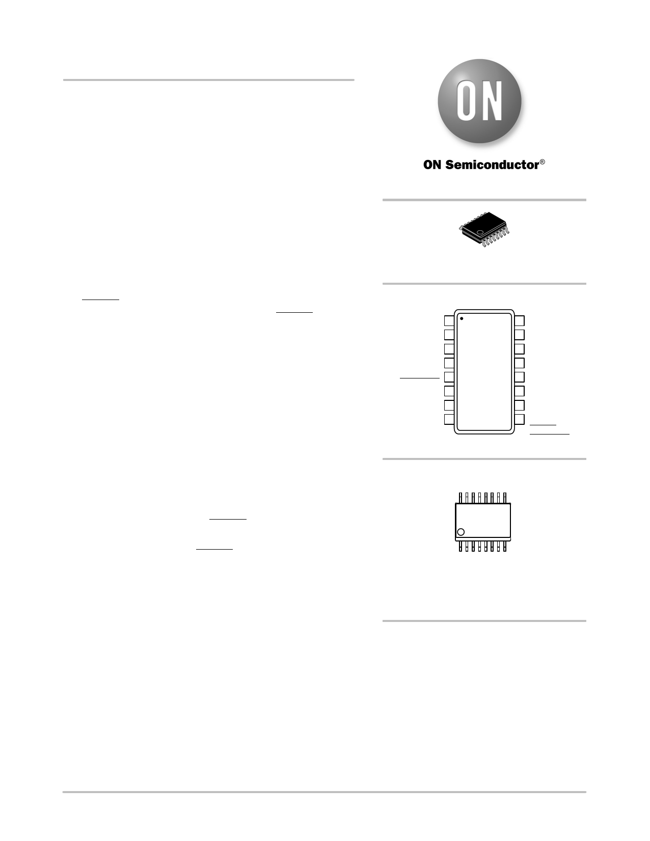
http://onsemi.com
QSOP−16
CASE 492
PIN ASSIGNMENT
SCL 1
GND 2
VCC 3
TACH3
PWM2/
SMBALERT
TACH1
4
5
6
TACH2 7
PWM3 8
ADT7467
(Top View)
16 SDA
15 PWM1/XTO
14 VCCP
13 D1+
12 D1−
11 D2+
10 D2−
9 TACH4/GPIO/
THERM/
SMBALERT
MARKING DIAGRAM
T7467A
RQZ
#YYWW
T7467ARQZ
#
YY
WW
= Specific Device Code
= Pb-Free Package
= Date Code
= Work Week
ORDERING INFORMATION
See detailed ordering and shipping information in the package
dimensions section on page 70 of this data sheet.
* For additional information on our Pb-Free strategy and soldering details, please
download the ON Semiconductor Soldering and Mounting Techniques
Reference Manual, SOLDERRM/D.
Semiconductor Components Industries, LLC, 2012
May, 2012 − Rev. 4
1
Publication Order Number:
ADT7467/D
1 page 
ADT7467
Table 3. ELECTRICAL SPECIFICATIONS (TA = TMIN to TMAX, VCC = VMIN to VMAX, unless otherwise noted.) (Note 1)
Parameter
Test Conditions/Comments
Min Typ Max
Unit
SMBus DIGITAL INPUTS (SCL, SDA)
Input High Voltage, VIH
Input Low Voltage, VIL
Hysteresis
2.0 −
−−
− 500
−V
0.4 V
− mV
DIGITAL INPUT LOGIC LEVELS (TACH INPUTS)
Input High Voltage, VIH
Maximum Input Voltage
2.0 −
−V
− − 5.5
Input Low Voltage, VIL
Minimum Input Voltage
−−
−0.3 −
0.8 V
−
Hysteresis
− 0.5 − V p−p
DIGITAL INPUT LOGIC LEVELS (THERM) ADTL+
Input High Voltage, VIH
Input Low Voltage, VIL
DIGITAL INPUT CURRENT
− 0.75 VCCP
−
− − 0.4
V
V
Input High Current, IIH
Input Low Current, IIL
Input Capacitance, CIN
SERIAL BUS TIMING
VIN = VCC
VIN = 0
−1 −
−−
−5
− mA
1 mA
− pF
Clock Frequency, fSCLK
10 − 400 kHz
Glitch Immunity, tSW
− − 50 ns
Bus Free Time, tBUF
4.7 −
− ms
Start Setup Time, tSU; STA
4.7 −
− ms
Start Hold Time, tHD; STA
4.0 −
− ms
SCL Low Time, tLOW
4.7 −
− ms
SCL High Time, tHIGH
4.0 −
50 ms
SCL, SDA Rise Time, tr
−
−
1000
ns
SCL, SDA Fall Time, tf
− − 300 ms
Data Setup Time, tSU; DAT
250 −
− ns
Data Hold Time, tHD; DAT
300 −
− ns
Detect Clock Low Timeout, tTIMEOUT
Can be Optionally Disabled
15 − 35 ms
1. All voltages are measured with respect to GND, unless otherwise specified. Typicals are at TA = 25C and represent the most likely
parametric norm. Logic inputs accept input high voltages up to VMAX even when the device is operating down to VMIN. Timing specifications
are tested at logic levels of VIL = 0.8 V for a falling edge and VIH = 2.0 V for a rising edge. SMBus timing specifications are guaranteed by
design and are not production tested.
SCL
SDA
tBUF
PS
t LOW
tR
tHD; STA
tHD; DAT
tF
tHIGH
tSU; DAT
t HD; STA
tSU; STA
S
Figure 2. Serial Bus Timing Diagram
tSU; STO
P
http://onsemi.com
5
5 Page 
ADT7467
Write Operations
The SMBus specification defines several protocols for
different types of read and write operations. The ones used
in the ADT7467 are discussed here. The following
abbreviations are used in Figure 18 through Figure 20:
S = start
P = stop
R = read
W = write
A = acknowledge
A = no acknowledge
The ADT7467 uses the following SMBus write protocols.
Send Byte
In this operation, the master device sends a single
command byte to a slave device as follows:
1. The master device asserts a start condition on
SDA.
2. The master sends the 7-bit slave address followed
by the write bit (low).
3. The addressed slave device asserts an
acknowledge on SDA.
4. The master sends a command code.
5. The slave asserts an acknowledge on SDA.
6. The master asserts a stop condition on SDA, and
the transaction ends.
For the ADT7467, the send byte protocol is used to write
a register address to RAM for a subsequent single byte read
from the same address. This operation is illustrated in
Figure 18.
12
3 4 56
S
Slave
Address
WA
Register
Address
AP
Figure 18. Setting a Register Address for
Subsequent Read
If the master is required to read data from the register
directly after setting up the address, it can assert a repeat start
condition immediately after the final acknowledge and carry
out a single byte read without asserting an intermediate stop
condition.
Write Byte
In this operation, the master device sends a command byte
and one data byte to the slave device as follows:
1. The master device asserts a start condition on
SDA.
2. The master sends the 7-bit slave address followed
by the write bit (low).
3. The addressed slave device asserts an
acknowledge on SDA.
4. The master sends a command code.
5. The slave asserts an acknowledge on SDA.
6. The master sends a data byte.
7. The slave asserts an acknowledge on SDA.
8. The master asserts a stop condition on SDA to end
the transaction.
This operation is illustrated in Figure 19.
12
3
S
Slave
Address
WA
4
Slave
Address
5 6 78
A Data A P
Figure 19. Single Byte Write to a Register
Read Operations
The ADT7467 uses the following SMBus read protocols.
Receive Byte
This operation is useful when repeatedly reading a single
register. The register address must have been set up
previously. In this operation, the master device receives a
single byte from a slave device as follows:
1. The master device asserts a start condition on
SDA.
2. The master sends the 7-bit slave address followed
by the read bit (high).
3. The addressed slave device asserts an
acknowledge on SDA.
4. The master receives a data byte.
5. The master asserts a no acknowledge on SDA.
6. The master asserts a stop condition on SDA, and
the transaction ends.
In the ADT7467, the receive byte protocol is used to read
a single byte of data from a register whose address has
previously been set by a send byte or write byte operation.
This operation is illustrated in Figure 20.
12
3 4 56
S
Slave
Address
RA
Data
AP
Figure 20. Single Byte Read from a Register
Alert Response Address
Alert response address (ARA) is a feature of SMBus
devices that allows an interrupting device to identify itself
to the host when multiple devices exist on the same bus.
The SMBALERT output can be used as either an interrupt
output or an SMBALERT. One or more outputs can be
connected to a common SMBALERT line connected to the
master. If a device’s SMBALERT line goes low, the
following procedure occurs:
1. SMBALERT is pulled low.
2. The master initiates a read operation and sends the
alert response address (ARA = 0001 100). This is
a general call address that must not be used as a
specific device address.
3. The device whose SMBALERT output is low
responds to the alert response address, and the
master reads its device address. The address of the
http://onsemi.com
11
11 Page | ||
| Páginas | Total 30 Páginas | |
| PDF Descargar | [ Datasheet ADT7467.PDF ] | |
Hoja de datos destacado
| Número de pieza | Descripción | Fabricantes |
| ADT7460 | dB COOL Remote Thermal Controller and Fan Controller | Analog Devices |
| ADT7461 | Temperature Monitor | Analog Devices |
| ADT7461 | Temperature Monitor | ON Semiconductor |
| ADT7461A | Temperature Monitor | ON Semiconductor |
| Número de pieza | Descripción | Fabricantes |
| SLA6805M | High Voltage 3 phase Motor Driver IC. |
Sanken |
| SDC1742 | 12- and 14-Bit Hybrid Synchro / Resolver-to-Digital Converters. |
Analog Devices |
|
DataSheet.es es una pagina web que funciona como un repositorio de manuales o hoja de datos de muchos de los productos más populares, |
| DataSheet.es | 2020 | Privacy Policy | Contacto | Buscar |