|
|
|
PDF DG9454E Data sheet ( Hoja de datos )
| Número de pieza | DG9454E | |
| Descripción | Analog Switch / Multiplexer | |
| Fabricantes | Vishay | |
| Logotipo | ||
Hay una vista previa y un enlace de descarga de DG9454E (archivo pdf) en la parte inferior de esta página. Total 13 Páginas | ||
|
No Preview Available !
www.vishay.com
DG9454E
Vishay Siliconix
Low Capacitance, +12 V / +5 V / +3 V, Triple SPDT (Triple 2:1)
Analog Switch / Multiplexer
DESCRIPTION
The DG9454E is a high precision triple SPDT (triple 2:1)
analog switch / multiplexer with enhanced performance on
low power consumption. The part features low parasitic
capacitance, low leakage, and low charge injection over the
full signal range which make it an ideal switch for healthcare,
data acquisition, and instrument products. Its compact size,
light weight, low power consumption, and low voltage
control capability are of advantages in portable consumer
applications such as goggles.
The DG9454E is designed to operate from a 3 V to 16 V
supply at V+, and 2.5 V to 5.5 V at VL, while guarantees
1.8 V logic compatible over the full operation voltage range.
Processed with advanced CMOS technology, the DG9454E
conducts equally well in both directions, offers rail to rail
analog signal handling and can be used both as a
multiplexer as well as a de-multiplexer.
The DG9454E operating temperature is specified
from -40 °C to +125 °C. It is available in ultra-compact
1.8 mm x 2.6 mm miniQFN16 package of lead (Pb)-free
nickel-palladium-gold device termination. It is represented
by the lead (Pb)-free “-E4” suffix. The nickel-palladium-gold
device terminations meet all JEDEC® standards for reflow
and MSL ratings.
FEATURES
• Operates with V+ = 3 V to 16 V,
VL = 2.5 V to 5.5 V
• Guaranteed 1.8 V logic control at full V+ range
• Low power consumption, both I+ and IL < 1 μA
• Low parasitic capacitance:
CD(ON): 8.8 pF
CD(OFF): 4 pF
CS(OFF): 3.1 pF
• High bandwidth: 356 MHz
• Low charge injection over the full signal range
• Compact miniQFN16 package
(1.8 mm x 2.6 mm x 0.55 mm)
• Material categorization: for definitions of
compliance please see www.vishay.com/doc?99912
APPLICATIONS
• Medical and healthcare systems
• Data acquisition systems
• Meters and instruments
• Games and Goggles
• Automatic test equipment
• Process control and automation
• Communication systems
• Battery powered systems
BENEFITS
• Low power consumption
• Precision switching
• Low voltage logic interface
• Bi-directional rail to rail signal switching
• Compact package option
• Extended operation temperature range
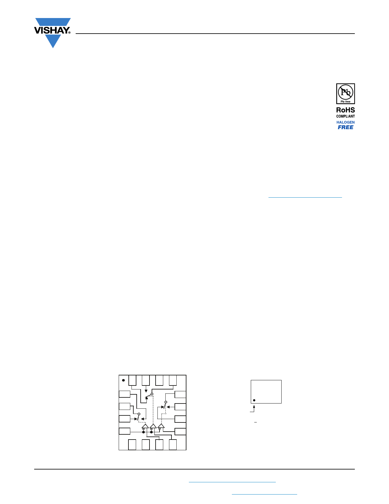
FUNCTIONAL BLOCK DIAGRAM AND PIN CONFIGURATION
DG9454E
mQFN-16
Y0 Y1 V+
Y
16 15 14 13
Z1 1
12 X
Yxx
Z2
Z0 3
Enable 4
11 X1
10 X0
9A
Pin 1
Device Marking:Jxx for DG9454E
(miniQFN16)
xx = Date/Lot Traceability Code
5 6 77
VL GND C
Top View
8
B
S16-0652-Rev. A, 18-Apr-16
1
Document Number: 67172
For technical questions, contact: [email protected]
THIS DOCUMENT IS SUBJECT TO CHANGE WITHOUT NOTICE. THE PRODUCTS DESCRIBED HEREIN AND THIS DOCUMENT
ARE SUBJECT TO SPECIFIC DISCLAIMERS, SET FORTH AT www.vishay.com/doc?91000
1 page 
www.vishay.com
DG9454E
Vishay Siliconix
SPECIFICATIONS FOR UNIPOLAR SUPPLIES
PARAMETER
Analog Switch
SYMBOL
TEST CONDITIONS
UNLESS OTHERWISE SPECIFIED
V+ = 5 V, VL = 2.7 V
VIN(A, B, C and enable) = 1.8 V, 0.5 V a
TEMP. b
TYP. c
-40 °C to +125 °C
MIN. d MAX. d
-40 °C to +85 °C
MIN. d MAX. d
UNIT
Analog Signal Range e
On-Resistance
VANALOG
RON
IS = 1 mA, VD = 0 V, 3.5 V
Full -
0
5
0 5V
Room 125
-
147
- 147
Full -
- 176 - 168
On-Resistance Match
RON
IS = 1 mA, VD = 3.5 V
Room 1.33
-
8
-8
Full -
-
8
-8
On-Resistance Flatness RFLATNESS
IS = 1 mA, VD = 0 V, 3 V
Room 21
-
31
- 31
Full - - 25 - 29
Switch Off
Leakage Current
IS(off)
V+ = 5.5 V, V- = 0 V
Room ± 0.03 -1 1 -1 1
Full - -50 50 -5 5
VD = 1 V / 4.5 V, VS = 4.5 V / 1 V Room ± 0.03 -1 1 -1 1
ID(off)
nA
Full - -50 50 -5 5
Channel On
Leakage Current
ID(on)
V+ = 5.5 V, V- = 0 V
VD = VS = 1 V / 4.5 V
Room ± 0.03 -1 1 -1 1
Full - -50 50 -5 5
Digital Control
VIN(A, B, C and enable) Low
VIN(A, B, C and enable) High
VIL
VIH
VL = 2.7 V
VL = 2.7 V
Full -
- 0.6 - 0.6
V
Full - 1.8 - 1.8 -
Input Current, VIN Low
Input Current, VIN High
IL
VIN(A, B, C and enable) under test = 0.6 V Full
0.02
-1
1
-1 1
μA
IH
VIN(A, B, C and enable) under test = 1.8 V Full
0.02
-1
1
-1 1
Dynamic Characteristics
Transition Time
tTRANS
Room 95 - 135 - 135
Full -
- 164 - 152
Enable Turn-On Time
Enable Turn-Off Time
tON
tOFF
RL = 300 , CL = 35 pF
see Fig. 1, 2, 3
Room 80 - 120 - 120
Full -
- 138 - 129
ns
Room 58
-
98
- 98
Full -
- 106 - 103
Break-Before-Make
Time Delay
tD
Room 45
-
-
--
Full - 24 - 15 -
Charge Injection e
Off Isolation e
Channel-to-Channel
Crosstalk e
Q
Vg = 0 V, Rg = 0 , CL = 1 nF
Full 1.44
-
- - - pC
OIRR
XTALK
RL = 50 , CL = 5 pF
f = 100 kHz
Room -95
-
-
--
dB
Room -92
-
-
--
Source Off Capacitance e
Drain Off Capacitance e
Channel On Capacitance e
Power Supply
CS(off)
CD(off)
CD(on)
f = 1 MHz
Room 3.5
-
-
--
Room 4.5
-
-
- - pF
Room 10.2
-
-
--
Power Supply Current
Ground Current
I+
IGND
Room 0.05
-
1
-1
Full - - 10 - 10
VIN(A, B, C and enable) = 0 V or 5 V
Room -0.05 -1
-
-1 -
μA
Full - -10 - -10 -
Logic Supply Current
IL
VL = 2.7 V
Room 0.05
-
1
-1
Full - - 10 - 10
Notes
a. VIN = input voltage to perform proper function.
b. Room = 25 °C, Full = as determined by the operating temperature suffix.
c. Typical values are for DESIGN AID ONLY, not guaranteed nor subject to production testing.
d. The algebraic convention whereby the most negative value is a minimum and the most positive a maximum, is used in this datasheet.
e. Guaranteed by design, not subject to production test.
S16-0652-Rev. A, 18-Apr-16
5
Document Number: 67172
For technical questions, contact: [email protected]
THIS DOCUMENT IS SUBJECT TO CHANGE WITHOUT NOTICE. THE PRODUCTS DESCRIBED HEREIN AND THIS DOCUMENT
ARE SUBJECT TO SPECIFIC DISCLAIMERS, SET FORTH AT www.vishay.com/doc?91000
5 Page 
www.vishay.com
miniQFN-16L
Package Information
Vishay Siliconix
D
(12) (11) (10) (9)
(13)
(14)
(15)
(16)
(1) (2) (3) (4)
(8)
(7)
(6)
(5)
be
(1) (2) (3) (4)
(16)
(15)
(14)
(13)
(12) (11) (10) (9)
BACK SIDE VIEW
(5)
(6)
(7)
(8)
MILLIMETERS
DIM
MIN.
NAM
A 0.70 0.75
A1 0
-
b 0.15 0.20
C 0.15 0.20
D 2.50 2.60
E 1.70 1.80
e 0.40 BSC
L 0.35 0.40
L1 0.45 0.50
ECN T16-0234-Rev. B, 09-May-16
DWG: 5954
MAX.
0.80
0.05
0.25
0.25
2.70
1.90
0.45
0.55
MIN.
0.0275
0
0.0059
0.0059
0.0984
0.0669
0.0137
0.0177
INCHES
NAM
0.0295
-
0.0078
0.0078
0.1023
0.0708
0.0157 BSC
0.0157
0.0196
MAX.
0.0315
0.002
0.0098
0.0098
0.1063
0.0748
0.0177
0.0216
Revision: 09-May-16
1 Document Number: 74323
THIS DOCUMENT IS SUBJECT TO CHANGE WITHOUT NOTICE. THE PRODUCTS DESCRIBED HEREIN AND THIS DOCUMENT
ARE SUBJECT TO SPECIFIC DISCLAIMERS, SET FORTH AT www.vishay.com/doc?91000
11 Page | ||
| Páginas | Total 13 Páginas | |
| PDF Descargar | [ Datasheet DG9454E.PDF ] | |
Hoja de datos destacado
| Número de pieza | Descripción | Fabricantes |
| DG9454 | Low Power Consumption Triple SPDT | Vishay Siliconix |
| DG9454E | Analog Switch / Multiplexer | Vishay |
| Número de pieza | Descripción | Fabricantes |
| SLA6805M | High Voltage 3 phase Motor Driver IC. |
Sanken |
| SDC1742 | 12- and 14-Bit Hybrid Synchro / Resolver-to-Digital Converters. |
Analog Devices |
|
DataSheet.es es una pagina web que funciona como un repositorio de manuales o hoja de datos de muchos de los productos más populares, |
| DataSheet.es | 2020 | Privacy Policy | Contacto | Buscar |