|
|
|
PDF A1369 Data sheet ( Hoja de datos )
| Número de pieza | A1369 | |
| Descripción | Customer Programmable Linear Hall-Effect Sensor Optimized | |
| Fabricantes | Allegro | |
| Logotipo | ||
Hay una vista previa y un enlace de descarga de A1369 (archivo pdf) en la parte inferior de esta página. Total 22 Páginas | ||
|
No Preview Available !
A1369
Customer Programmable Linear Hall-Effect Sensor
Optimized for Use in Current Sensing Applications
FEATURES AND BENEFITS
• Customer programmable offset, and sensitivity
• Sensitivity & QVO temperature coefficients programmed
at Allegro for improved accuracy
• Output value decreases with South Magnetic Field and
increases with North Magnetic field.
• 3-pin SIP package for easy integration with magnetic
concentrator
• Low noise, moderate bandwidth, analog output
• High speed chopping scheme minimizes QVO drift over
temperature
• Temperature-stable quiescent voltage output and
sensitivity
• Precise recoverability after temperature cycling
• Output voltage clamps provide short circuit diagnostic
capabilities
• Under voltage lock-out (UVLO)
Continued on the next page…
Package: 3-Pin SIP (suffix UA)
Not to scale
DESCRIPTION
The Allegro™ A1369 is a customer programmable, high
accuracy linear Hall effect-based current sensor IC. It is
packaged in a thin 3-pin SIPpackage to allow for easy integration
with a magnetic core to create a highly accurate current sensing
module. The programmable nature of the A1369 enables it
to account for manufacturing tolerances in the final current
sensing module assembly.
This temperature-stable device is available in a through-hole
single in-line package (TO-92). The accuracy of the device
is enhanced via programmability on the output pin for end-
of-line optimization without the added complexity and cost of
a fully programmable device. The device features One-Time-
Programming (OTP), using non-volatile memory, to optimize
device sensitivity and the quiescent output voltage (QVO)
(output with no magnetic field) for a given application or
circuit. The A1369 also allow for optimized performance over
temperature through programming the temperature coefficient
for both Sensitivity and QVO at Allegro end of line test.
These ratiometric Hall effect sensor ICs provide a voltage
output that is proportional to the applied magnetic field. The
quiescent voltage output is user adjustable around 50% of the
supply voltage and the output sensitivity is programmable
within a range of 8.5 mV/G to 12.5 mV/G for the A1369-10
and 22 mV/G to 26 mV/G for the A1369-24.
Continued on the next page…
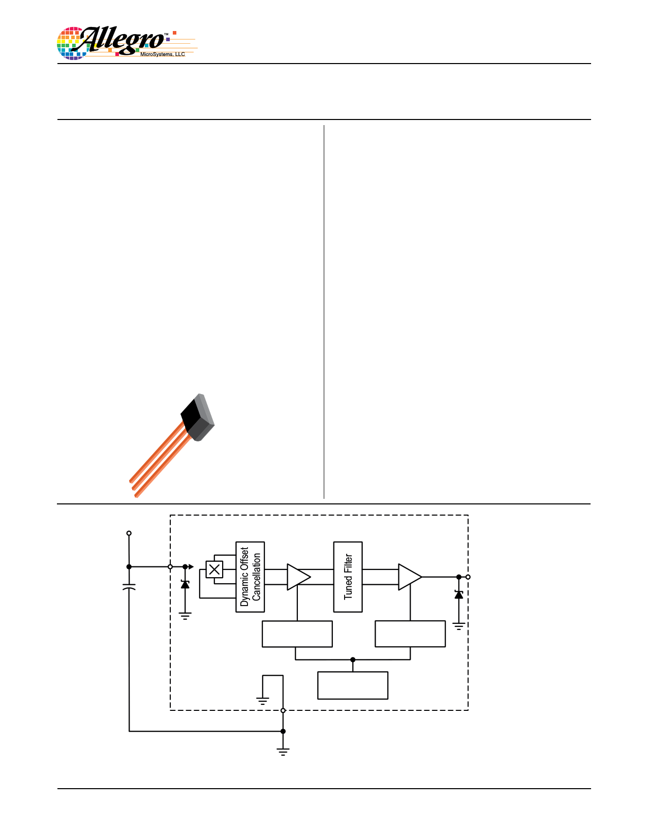
V+
VCC
VOUT/
Programming
Sensitivity and
Sensitivity TC
Offset and
Offset TC
Trim Control
GND
A1369-DS, Rev. 1
Functional Block Drawing
1 page 
A1369
Customer Programmable Linear Hall-Effect Sensor
Optimized for Use in Current Sensing Applications
ELECTRICAL CHARACTERISTICS (continued): valid over TA, CBYPASS = 0.1 µF, VCC = 5 V, unless otherwise noted
Characteristic
Symbol
Test Conditions
Min.
Typ.
Max.
Unit
Customer Quiescent Voltage Output Programming
Guaranteed Quiescent Voltage Output
Range7
VOUT(Q)
TA = 25ºC
2.45 – 2.55 V
Quiescent Voltage Output
Programming Bits
− 5 – Bits
Average Quiescent Voltage Output
Step Size8,9
StepVOUT(Q) TA = 25ºC
4.75 7.5 10.5 mV
Quiescent Voltage Output
Programming Resolution10
ErrPGVOUT(Q) TA = 25ºC
–
StepVOUT(Q)
× ±0.5
Customer Sensitivity Programming
Sensitivity Programming Bits
– 7 – Bits
Default Sensitivity
Guaranteed Fine Step Sensitivity
Range11
Average Sensitivity Step Size8,9
Sens
Sens
StepSens
A1369-10, TA = 25ºC
A1369-24, TA = 25ºC
A1369-10, TA = 25ºC
A1369-24, TA = 25ºC
A1369-10, TA = 25ºC
A1369-24, TA = 25ºC
Sensitivity Programming Resolution10 ErrPROGSENS TA = 25ºC
−
−
-8.5
-22
-72
-163
–
-10.5
-24
–
–
-102
-233
StepSens
× ±0.5
−
−
-12.5
-26
-133
-303
–
mV/G
mV/G
mV/G
mV/G
µV/G
µV/G
µV/G
Customer Clamp Disable Programming
Clamp Disable Bit
– 1 – Bit
Output Voltage12
Customer Lock
VSAT,HIGH
VSAT,LOW
B = -X G;
RL = 4.7 kΩ (VOUT to GND)
B = + X G;
RL = 4.7 kΩ (VOUT to GND)
4.75 – – V
– – 0.25 V
Overall Programming Lock Bit
LOCK
– 1 – Bit
Continued on the next page…
7VOUT(Q)(max) is the value available with all programming fuses blown (maximum programming code set). VOUT(Q) is the total range from VOUT(Q)init up to and includ-
ing VOUT(Q)(max). See Characteristic Definitions.
8Step size is larger than required to account for manufacturing spread. See Characteristics Definitions
9Non-ideal behavior in the programming DAC can cause the step size at each significant bit rollover code to be twice the maximum specified value of StepVOUT(Q) or
StepSENS
10Fine programming value accuracy. See Characteristic Definitions
11Sens(max) is the value available with all programming fuses blown (maximum programming code set). Sens range is the total range from Sensinit up to and including
Sens(max). See Characteristic Definitions.
12 VSAT,HIGH and VVSAT,LOW will scale with the supply voltage due to the Ratiometry of the part
Allegro MicroSystems, LLC
115 Northeast Cutoff
Worcester, Massachusetts 01615-0036 U.S.A.
1.508.853.5000; www.allegromicro.com
5
5 Page 
A1369
Customer Programmable Linear Hall-Effect Sensor
Optimized for Use in Current Sensing Applications
PROGRAMMING GUIDELINES
Overview
Programming is accomplished by sending a series of input volt-
age pulses serially through the VOUT pin of the device. A unique
combination of different voltage level pulses controls the internal
programming logic of the device to select a desired programma-
ble parameter and change its value. There are three voltage levels
that must be taken into account when programming. These levels
are referred to as high (VPH), mid (VPM), and low (VPL).
The A1369 features a Try mode, Blow mode, and Read mode:
• In Try mode, the value of multiple programmable parameters
may be set and measured simultaneously. The parameter
values are stored temporarily, and reset after cycling the
supply voltage.
• In Blow mode, the value of a single programmable parameter
may be permanently set by blowing solid-state fuses
internal to the device. Additional parameters may be blown
sequentially. This mode is used for blowing the device-level
fuse, which permanently blocks the further programming of all
parameters. Device locking is also accomplished in this mode.
• In Read mode, the current state of the programming fuses can
be read back for verification of programmed value.
The programming sequence is designed to help prevent the device
from being programmed accidentally; for example, as a result
of noise on the supply line. Although any programmable vari-
able power supply can be used to generate the pulse waveforms,
Allegro highly recommends using the Allegro Sensor Evaluation
Kit, available on the Allegro Web site On-line Store. The manual
for that kit is available for
Definition of Terms
Register. The section of the programming logic that controls the
choice of programmable modes and parameters.
Bit Field. The internal fuses unique to each register, represented
as a binary number. Incrementing the bit field of a particular
register causes its programmable parameter to change, based on
the internal programming logic.
Key. A series of mid-level voltage pulses used to select a register,
with a value expressed as the decimal equivalent of the binary
value. The LSB of a register is denoted as key 1, or bit 0.
Code. The number used to identify the combination of fuses
activated in a bit field, expressed as the decimal equivalent of the
binary value. The LSB of a bit field is denoted as code 1, or bit 0.
Addressing. Incrementing the bit field code of a selected register
by serially applying a pulse train through the VCC pin of the
device. Each parameter can be measured during the addressing
process, but the internal fuses must be blown before the program-
ming code (and parameter value) becomes permanent.
Fuse Blowing. Applying a high voltage pulse of sufficient
duration to permanently set an addressed bit by blowing a fuse
internal to the device. Once a bit (fuse) has been blown, it cannot
be reset.
Blow Pulse. A high voltage pulse of sufficient duration to blow
the addressed fuse.
Cycling the Supply. Powering-down, and then powering-up the
supply voltage. Cycling the supply is used to clear the program-
ming settings in Try mode.
Allegro MicroSystems, LLC
115 Northeast Cutoff
Worcester, Massachusetts 01615-0036 U.S.A.
1.508.853.5000; www.allegromicro.com
11
11 Page | ||
| Páginas | Total 22 Páginas | |
| PDF Descargar | [ Datasheet A1369.PDF ] | |
Hoja de datos destacado
| Número de pieza | Descripción | Fabricantes |
| A1360 | PNP Transistor - 2SA1360 | Toshiba |
| A1360 | Low-Noise Programmable Linear Hall Effect Sensor ICs | Allegro |
| A1361 | Low-Noise Programmable Linear Hall Effect Sensor ICs | Allegro |
| A1362 | Low-Noise Programmable Linear Hall Effect Sensor ICs | Allegro |
| Número de pieza | Descripción | Fabricantes |
| SLA6805M | High Voltage 3 phase Motor Driver IC. |
Sanken |
| SDC1742 | 12- and 14-Bit Hybrid Synchro / Resolver-to-Digital Converters. |
Analog Devices |
|
DataSheet.es es una pagina web que funciona como un repositorio de manuales o hoja de datos de muchos de los productos más populares, |
| DataSheet.es | 2020 | Privacy Policy | Contacto | Buscar |