|
|
PDF CD4053BC Data sheet ( Hoja de datos )
| Número de pieza | CD4053BC | |
| Descripción | Triple 2-Channel Analog Multiplexer/Demultiplexer | |
| Fabricantes | Fairchild Semiconductor | |
| Logotipo | ||
Hay una vista previa y un enlace de descarga de CD4053BC (archivo pdf) en la parte inferior de esta página. Total 13 Páginas | ||
|
No Preview Available !
November 1983
Revised April 2002
CD4051BC • CD4052BC • CD4053BC
Single 8-Channel Analog Multiplexer/Demultiplexer •
Dual 4-Channel Analog Multiplexer/Demultiplexer •
Triple 2-Channel Analog Multiplexer/Demultiplexer
General Description
The CD4051BC, CD4052BC, and CD4053BC analog mul-
tiplexers/demultiplexers are digitally controlled analog
switches having low “ON” impedance and very low “OFF”
leakage currents. Control of analog signals up to 15Vp-p
can be achieved by digital signal amplitudes of 3−15V. For
example, if VDD = 5V, VSS = 0V and VEE = −5V, analog sig-
nals from −5V to +5V can be controlled by digital inputs of
0−5V. The multiplexer circuits dissipate extremely low qui-
escent power over the full VDD−VSS and VDD−VEE supply
voltage ranges, independent of the logic state of the control
signals. When a logical “1” is present at the inhibit input ter-
minal all channels are “OFF”.
CD4051BC is a single 8-channel multiplexer having three
binary control inputs. A, B, and C, and an inhibit input. The
three binary signals select 1 of 8 channels to be turned
“ON” and connect the input to the output.
CD4052BC is a differential 4-channel multiplexer having
two binary control inputs, A and B, and an inhibit input. The
two binary input signals select 1 or 4 pairs of channels to
be turned on and connect the differential analog inputs to
the differential outputs.
CD4053BC is a triple 2-channel multiplexer having three
separate digital control inputs, A, B, and C, and an inhibit
input. Each control input selects one of a pair of channels
which are connected in a single-pole double-throw configu-
ration.
Features
s Wide range of digital and analog signal levels:
digital 3 – 15V, analog to 15Vp-p
s Low “ON” resistance: 80Ω (typ.) over entire 15Vp-p
signal-input range for VDD − VEE = 15V
s High “OFF” resistance:
channel leakage of ±10 pA (typ.) at VDD − VEE = 10V
s Logic level conversion for digital addressing signals of
3 – 15V (VDD − VSS = 3 – 15V) to switch analog signals
to 15 Vp-p (VDD − VEE = 15V)
s Matched switch characteristics:
∆RON = 5Ω (typ.) for VDD − VEE = 15V
s Very low quiescent power dissipation under all
digital-control input and supply conditions:
1 µ W (typ.) at VDD − VSS = VDD − VEE = 10V
s Binary address decoding on chip
Ordering Code:
Order Number Package Number
Package Description
CD4051BCM
M16A
16-Lead Small Outline Integrated Circuit (SOIC), JEDEC MS-012, 0.150" Narrow
CD4051BCSJ
M16D
16-Lead Small Outline Package (SOP), EIAJ TYPE II, 5.3mm Wide
CD4051BCMTC
MTC16
16-Lead Thin Shrink Small Outline Package (TSSOP), JEDEC MO-153, 4.4mm Wide
CD4051BCN
N16E
16-Lead Plastic Dual-In-Line Package (PDIP), JEDEC MS-001, 0.300" Wide
CD4052BCM
M16A
16-Lead Small Outline Integrated Circuit (SOIC), JEDEC MS-012, 0.150" Narrow
CD4052BCSJ
M16D
16-Lead Small Outline Package (SOP), EIAJ TYPE II, 5.3mm Wide
CD4052BCN
N16E
16-Lead Plastic Dual-In-Line Package (PDIP), JEDEC MS-001, 0.300" Wide
CD4053BCM
M16A
16-Lead Small Outline Integrated Circuit (SOIC), JEDEC MS-012, 0.150" Narrow
CD4053BCSJ
M16D
16-Lead Small Outline Package (SOP), EIAJ TYPE II, 5.3mm Wide
CD4053BCN
N16E
16-Lead Plastic Dual-In-Line Package (PDIP), JEDEC MS-001, 0.300" Wide
Devices also available in Tape and Reel. Specify by appending the suffix letter “X” to the ordering code.
© 2002 Fairchild Semiconductor Corporation DS005662
www.fairchildsemi.com
1 page 
Absolute Maximum Ratings(Note 1)
DC Supply Voltage (VDD)
Input Voltage (VIN)
Storage Temperature
Range (TS)
Power Dissipation (PD)
Dual-In-Line
Small Outline
Lead Temperature (TL)
(soldering, 10 seconds)
−0.5 VDC to +18 VDC
−0.5 VDC to VDD +0.5 VDC
−65°C to +150°C
700 mW
500 mW
260°C
Recommended Operating
Conditions
DC Supply Voltage (VDD)
Input Voltage (VIN)
Operating Temperature Range (TA)
CD4051BC/CD4052BC/CD4053BC
+5 VDC to +15 VDC
0V to VDD VDC
−55°C to +125°C
Note 1: “Absolute Maximum Ratings” are those values beyond which the
safety of the device cannot be guaranteed. Except for “Operating Tempera-
ture Range” they are not meant to imply that the devices should be oper-
ated at these limits. The Electrical Characteristics tables provide conditions
for actual device operation.
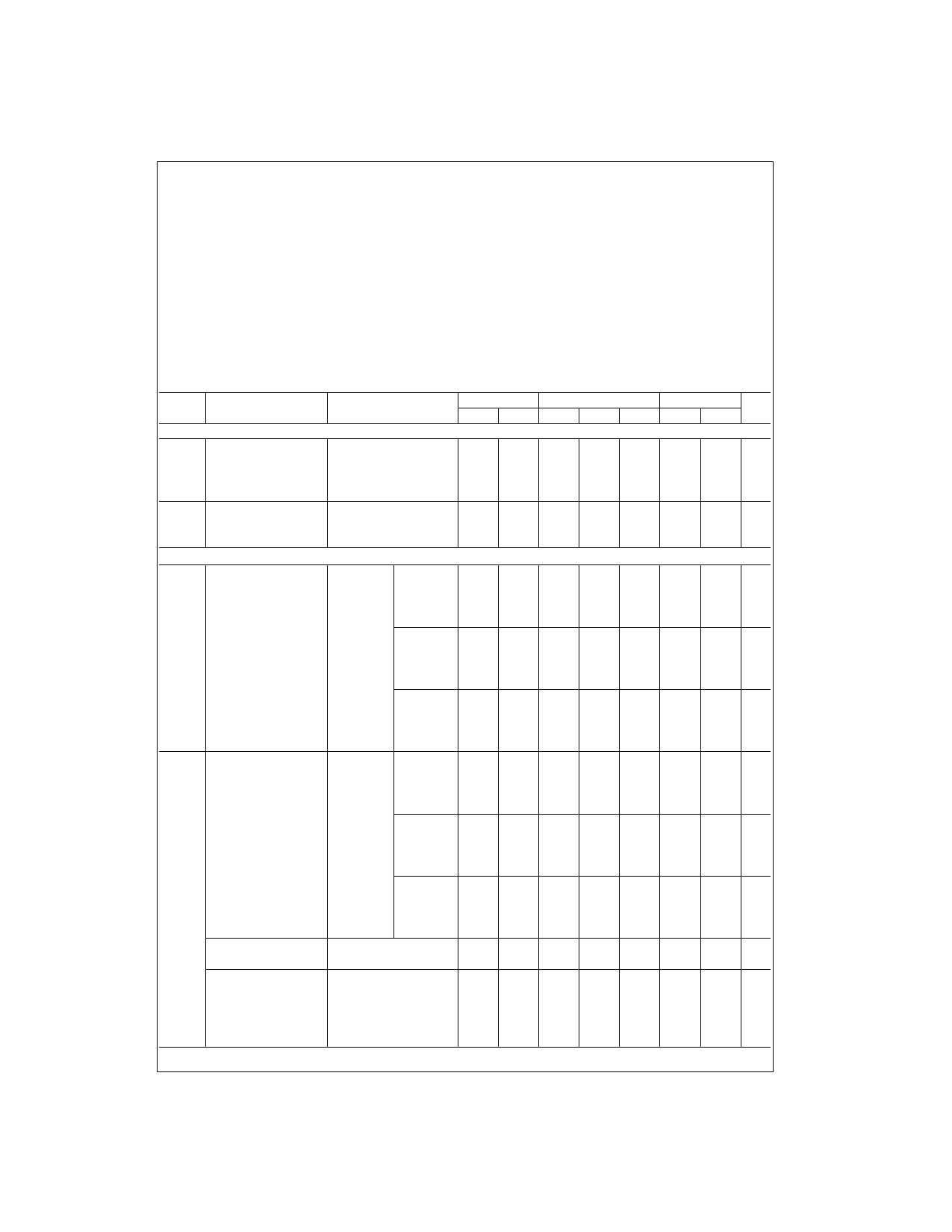
DC Electrical Characteristics (Note 2)
Symbol
Parameter
Conditions
−55°C
+25°
125°C
Units
Min Max Min Typ Max Min Max
Control A, B, C and Inhibit
IIN Input Current
VDD = 15V,
VEE = 0V
VIN = 0V
VDD = 15V,
VEE = 0V
VIN = 15V
IDD Quiescent Device Current VDD = 5V
VDD = 10V
VDD = 15V
−0.1
0.1
5
10
20
−10−5
−0.1
10−5
0.1
5
10
20
−1.0
µA
1.0
150
300 µA
600
Signal Inputs (VIS) and Outputs (VOS)
RON
“ON” Resistance (Peak
RL = 10 kΩ VDD = 2.5V,
for VEE ≤ VIS ≤ VDD)
(any channel VEE = −2.5V
selected)
or VDD = 5V,
VEE = 0V
VDD = 5V,
VEE = −5V
or VDD = 10V,
VEE = 0V
VDD = 7.5V,
VEE = −7.5V
or VDD = 15V,
VEE = 0V
∆RON
∆ “ON” Resistance
RL = 10 kΩ VDD = 2.5V,
Between Any Two
(any channel VEE = −2.5V
Channels
selected)
or VDD = 5V,
VEE = 0V
VDD = 5V
VEE = −5V
or VDD = 10V,
VEE = 0V
VDD = 7.5V,
VEE = −7.5V
or VDD = 15V,
VEE = 0V
“OFF” Channel Leakage VDD=7.5V,
VEE=−7.5V
Current, any channel “OFF” O/I=±7.5V, I/O=0V
800
310
200
±50
270 1050
120 400
80 240
10
10
5
±0.01 ±50
1300 Ω
550 Ω
320 Ω
Ω
Ω
Ω
±500 nA
“OFF” Channel Leakage Inhibit = 7.5V CD4051
±200
±0.08 ±200
±2000
Current, all channels
“OFF” (Common
OUT/IN)
VDD = 7.5V,
VEE = −7.5V,
O/I = 0V
D4052
±200
±0.04 ±200
±2000 nA
I/O = ±7.5V CD4053
±200
±0.02 ±200
±2000
5 www.fairchildsemi.com
5 Page 
Physical Dimensions inches (millimeters) unless otherwise noted (Continued)
16-Lead Small Outline Package (SOP), EIAJ TYPE II, 5.3mm Wide
Package Number M16D
11 www.fairchildsemi.com
11 Page | ||
| Páginas | Total 13 Páginas | |
| PDF Descargar | [ Datasheet CD4053BC.PDF ] | |
Hoja de datos destacado
| Número de pieza | Descripción | Fabricantes |
| CD4053B | CMOS Analog Multiplexers / Demultiplexers | RCA |
| CD4053B | (CD4051BE - CD4053BE) CMOS Analog Multiplexers / Demultiplexers | Harris Semiconductor |
| CD4053B | CMOS Single 8-Channel Analog Multiplexer/Demultiplexer With Logic-Level Conversion (Rev. H) | Texas Instruments |
| CD4053B-Q1 | CMOS Analog Multiplexer/Demulitiplexer With Logic-Level Conversion (Rev. A) | Texas Instruments |
| Número de pieza | Descripción | Fabricantes |
| SLA6805M | High Voltage 3 phase Motor Driver IC. |
Sanken |
| SDC1742 | 12- and 14-Bit Hybrid Synchro / Resolver-to-Digital Converters. |
Analog Devices |
|
DataSheet.es es una pagina web que funciona como un repositorio de manuales o hoja de datos de muchos de los productos más populares, |
| DataSheet.es | 2020 | Privacy Policy | Contacto | Buscar |
