|
|
|
PDF CLC5903 Data sheet ( Hoja de datos )
| Número de pieza | CLC5903 | |
| Descripción | Dual Digital Tuner / AGC | |
| Fabricantes | National Semiconductor | |
| Logotipo | ||
Hay una vista previa y un enlace de descarga de CLC5903 (archivo pdf) en la parte inferior de esta página. Total 29 Páginas | ||
|
No Preview Available !
June 2004
N National Semiconductor
CLC5903
Dual Digital Tuner / AGC
0
0
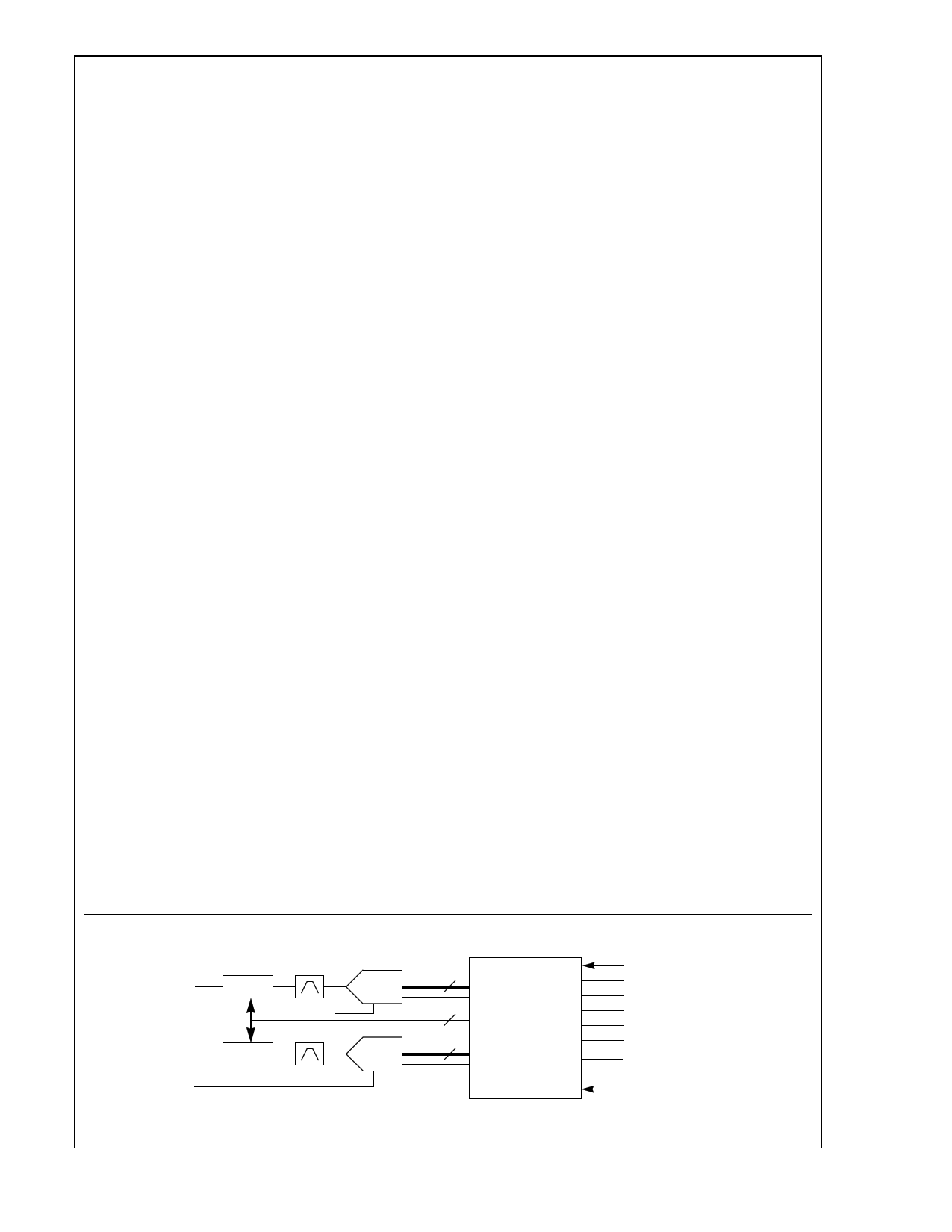
General Overview
The CLC5903 Dual Digital Tuner / AGC IC is a two channel
digital downconverter (DDC) with integrated automatic gain
control (AGC). The CLC5903 is a key component in the
Enhanced Diversity Receiver Chipset (EDRCS) which
includes one CLC5903 Dual Digital Tuner / AGC, two
CLC5957 12-bit analog-to-digital converters (ADCs), and two
CLC5526 digitally controlled variable gain amplifiers
(DVGAs). This system allows direct IF sampling of signals up
to 300MHz for enhanced receiver performance and reduced
system costs.
The CLC5903 is an enhanced replacement for the CLC5902
in the Diversity Receiver Chipset (DRCS). The main
improvements relative to the CLC5902 are a 50% increase in
maximum sample rate from 52MHz to 78MHz, a 62%
reduction in power consumption from 760mW to 290mW,
and the added flexibility to independently program filter
coefficients in the two channels. A block diagram for a
DRCS-based narrowband communications system is shown
in Figure 1.
The CLC5903 offers high dynamic range digital tuning and
filtering based on hard-wired digital signal processing (DSP)
technology. Each channel has independent tuning, phase
offset, filter coefficients, and gain settings. Channel filtering
is performed by a series of three filters. The first is a 4-stage
Cascaded Integrator Comb (CIC) filter with a programmable
decimation ratio from 8 to 2048. Next there are two
symmetric FIR filters, a 21-tap and a 63-tap, both with
independent programmable coefficients. The first FIR filter
decimates the data by 2, the second FIR decimates by either
2 or 4. Channel filter bandwidth at 52MSPS ranges from
±650kHz down to ±1.3kHz. At 78MSPS, the maximum
bandwidth increases to ±975kHz.
The CLC5903’s AGC controller monitors the ADC output and
controls the ADC input signal level by adjusting the DVGA
setting. AGC threshold, deadband+hysteresis, and the loop
time constant are user defined. Total dynamic range of
greater than 120dB full-scale signal to noise in a 200kHz
bandwidth can be achieved with the Diversity Receiver
Chipset.
Features
78MSPS Operation
Low Power, 145mW/channel, 52 MHz, Dec=192
Two Independent Channels with 14-bit inputs
Serial Daisy-chain Mode for quad receivers
Greater than 100 dB image rejection
Greater than 100 dB spurious free dynamic range
0.02 Hz tuning resolution
User Programmable AGC with enhanced Power Detector
Channel Filters include a Fourth Order CIC followed by
21-tap and 63-tap Symmetric FIRs
FIR filters process 21-bit Data with 16-bit Programmable
Coefficients
Two independent FIR coefficient memories which can be
routed to either or both channels.
Flexible output formats include 12-bit Floating Point or 8,
16, 24, and 32 bit Fixed Point
Serial and Parallel output ports
JTAG Boundary Scan
8-bit Microprocessor Interface
128 pin PQFP and 128 pin FBGA packages
100% Software compatible with the CLC5902
Pin compatible with the CLC5902 except for VDD voltage
Applications
Cellular Basestations
Satellite Receivers
Wireless Local Loop Receivers
Digital Communications
IF A
IF B
CLK
CLC5526
DVGA
LC
DVGA
LC
CLC5957
ADC
DAV
12
8
ADC
12
DAV
CLC5903
Dual Digital
Tuner/AGC
Figure 1. Diversity Receiver Chipset Block Diagram
SCK_IN
SerialOutA/B
SerialOutB
SCK
SFS
RDY
ParallelOutput[15..0]
ParallelOutputEnable
ParallelSelect[2..0]
©2004 National Semiconductor Corporation DS200286
www.national.com
Revision 1.6
1 page 
AC Characteristics (Continued)
(FS=78MHz, CIC Decimation=48, F2 Decimation=2; unless specified)
Symbol
Parameter (CL=50pF)
Min
tCSPW
tCDLY
tCZ
IDD
IDDIO
Controlling strobe pulse width (Write) (Figure 15)
Control output delay controlling signal low to D (Read) (Figure 15)
Control tri-state delay after controlling signal high (Figure 15)
Dynamic Supply Current (FCK =78MHz, N=48, SCK=39MHz)
Dynamic Supply Current (FCK =78MHz, N=48, SCK=39MHz)
30
Note 1: Datasheet min/max specification limits are guaranteed by design, test, or statistical analysis.
Note 2: All output pins provide 16mA output drive except TDO (pin 116) which provides 4mA output drive.
Note 3: tSFSV refers to the rising edge of SCK when SCK_POL=0 and the falling edge when SCK_POL=1.
Note 4: tOV refers to the rising edge of SCK when SCK_POL=0 and the falling edge when SCK_POL=1.
Note 5: tRDYV refers to the rising edge of RDY when RDY_POL=0 and the falling edge when RDY_POL=1.
Typ
120
65
Max
30
20
200
100
Units
ns
ns
ns
mA
mA
CLC5903SM Pinout
A1
AIN12
B1
AIN10
C1
AIN7
D1
AIN5
E1
AIN2
F1
VSS
G1
VDD
H1
BIN10
J1
BIN7
K1
BIN4
L1
BIN1
M1
NC
A2
VDDIO
B2
VSSIO
A3 A4
AGAIN1 SCAN_EN
B3 B4
NC TRST
A5
TCK
B5
TMS
A6 A7 A8 A9
VDD POUT_SEL1 VSSIO VDDIO
B6 B7 B8 B9
TDO POUT_SEL0 POUT_EN POUT4
A10
POUT3
B10
NC
A11
NC
B11
SCK_IN
A12
NC
B12
POUT5
C2
AIN11
C3 C4
C5
NC ASTROB VSS
C6 C7 C8 C9 C10 C11 C12
TDI POUT0 POUT2 NC VSSIO POUT6 POUT8
D2
AIN8
E2
AIN1
F2
CKA
D3
AIN13
E3
AIN6
F3
AIN3
D4 D5 D6 D7
AGAIN2 AGAIN0 POUT_SEL2 POUT1
E4
AIN9
F4
AIN4
D8 D9 D10 D11 D12
VSS POUT7 VDDIO POUT11 POUT10
E9 E10 E11 E12
POUT9 VSSIO POUT13 POUT12
F9 F10 F11 F12
SFS POUT14 VDD POUT15
G2
BIN13
G3
BIN12
G4
AIN0
G9 G10 G11 G12
RDY BOUT VSSIO AOUT
H2 H3 H4
BIN11
BIN9
BIN5
H9 H10 H11 H12
D[2] D[0]
SCK VDDIO
J2 J3 J4 J5 J6 J7 J8 J9 J10 J11 J12
BIN8
BIN6
BIN3 BGAIN2
SI
NC
CE
D[7] VSSIO
D[1]
VSS
K2 K3 K4 K5 K6 K7 K8 K9 K10 K11 K12
BIN2 BIN0 CKB BSTROB VSSIO A[4] A[1] RD NC D[4] VDD
L2 L3 L4 L5 L6 L7 L8 L9 L10 L11 L12
VSS NC BGAIN1 NC A[6] A[5] A[3] A[0] D[6] NC D[3]
M2 M3 M4 M5 M6 M7 M8 M9 M10 M11 M12
VDDIO BGAIN0
MR
A[7] VDD
VSS
A[2]
WR
VSSIO VDDIO
D[5]
Top View
Figure 3. CLC5903SM FBGA Pinout
5 www.national.com
5 Page 
TCK
TDO
TCK
TDI, TDS
TCK
D
TCK
D
CE
WR
RD
A[7:0]
D[7:0]
CE
WR
RD
A[7:0]
D[7:0]
CE
WR
A[7:0]
D[7:0]
CE
WR
A[7:0]
D[7:0]
tJPCO
tJPEN
tJCL
tJPSU
tJPDZ
tJCH
tJPH
tJSCO
tJSEN
tJSDZ
tJSSU
tJSH
Figure 14. CLC5903 JTAG Port Timing
tCSU
tCDLY
READ CYCLE; NORMAL MODE
tCSU
tCSPW
WRITE CYCLE; NORMAL MODE
tCSU
tCDLY
READ CYCLE; RD HELD LOW
tCSPW
tCSU
WRITE CYCLE; RD HELD LOW
Figure 15. CLC5903 Control I/O Timing
11
tCHD
tCZ
tCHD
tCHD
tCZ
tCHD
www.national.com
11 Page | ||
| Páginas | Total 29 Páginas | |
| PDF Descargar | [ Datasheet CLC5903.PDF ] | |
Hoja de datos destacado
| Número de pieza | Descripción | Fabricantes |
| CLC5902 | Dual Digital Tuner/AGC | National Semiconductor |
| CLC5902VLA | Dual Digital Tuner/AGC | National Semiconductor |
| CLC5903 | Dual Digital Tuner / AGC | National Semiconductor |
| CLC5903 | CLC5903 Dual Digital Tuner/AGC (Rev. D) | Texas Instruments |
| Número de pieza | Descripción | Fabricantes |
| SLA6805M | High Voltage 3 phase Motor Driver IC. |
Sanken |
| SDC1742 | 12- and 14-Bit Hybrid Synchro / Resolver-to-Digital Converters. |
Analog Devices |
|
DataSheet.es es una pagina web que funciona como un repositorio de manuales o hoja de datos de muchos de los productos más populares, |
| DataSheet.es | 2020 | Privacy Policy | Contacto | Buscar |