|
|
|
PDF CLC5665IMX Data sheet ( Hoja de datos )
| Número de pieza | CLC5665IMX | |
| Descripción | Low Distortion Amplifier with Disable | |
| Fabricantes | National Semiconductor | |
| Logotipo | ||
Hay una vista previa y un enlace de descarga de CLC5665IMX (archivo pdf) en la parte inferior de esta página. Total 8 Páginas | ||
|
No Preview Available !
N
CLC5665
Low Distortion Amplifier with Disable
June 1999
General Description
The CLC5665 is a low-cost, wideband amplifier that provides very
low 2nd and 3rd harmonic distortion at 1MHz (-89/-92dBc). The
great slew rate of 1800V/µs, bandwidth of 90MHz (Av = +1) and
fast disable make it an excellent choice for many high speed
multiplexing applications. Like all current feedback op amps, the
CLC5665 allows the frequency response to be optimized
(or adjusted) by the selection of the feedback resistor. For
demanding video applications, the 0.1dB bandwidth to 20MHz
and differential gain/phase of 0.05%/0.05° make the CLC5665
the preferred component for broadcast quality NTSC and PAL
video systems.
The large voltage swing (28Vpp), continuous output current
(85mA) and slew rate (1800V/µs) provide high-fidelity signal
conditioning for applications such as CCDs, transmission lines
and low impedance circuits.
xDSL, video distribution, multimedia and general purpose
applications will benefit from the CLC5665’s wide bandwidth and
disable feature. Power is reduced and the output becomes a high
impedance when disabled. The wide gain range of the CLC5665
makes this general purpose op amp an improved solution for
circuits such as active filters, single-to-differential-ended drivers,
DAC transimpedance amplifiers and MOSFET drivers.
Features
s 0.1dB gain flatness to 20MHz (Av = +2)
s 90MHz bandwidth (Av = +1)
s Large signal BW 25MHz
s 1800V/µs slew rate
s 0.05%/0.05° differential gain/phase
s ±5V, ±15V or single supplies
s 200ns disable to high-impedance output
s Wide gain range
s -89/-92dBc HD2/HD3 (RL = 500Ω)
s Low cost
Applications
s xDSL driver
s Twisted pair driver
s Cable driver
s Video distribution
s CCD clock driver
s Multimedia systems
s DAC output buffers
s Imaging systems
Non-Inverting Frequency Response
Gain
Av = 1
Rf = 698
Phase
Av = 50
Av = 10
Rf = 100 Av = 2
Rf = 604
Av = 1
Av = 50
Rf = 500
Av = 2
Av = 10
0
-45
-90
-135
-180
1 10 100
Frequency (MHz)
+
Vin (Vpp)
-
DIS
+
CLC5665
-
Rf1
Rg 604Ω
1.2kΩ
Rf2
604Ω
-
CLC5665
+
Typical Application
Differential Line Driver for xDSL
Ro
Vo = 2Vin
1:n
nVo
RL
Ro
Note: Supply and Bypassing not shown.
DIS
© 1999 National Semiconductor Corporation
Printed in the U.S.A.
Pinout
DIP & SOIC
NC 1
Vinv 2
Vnon-inv 3
-Vcc 4
-
+
8 DIS
7 +Vcc
6 Vout
5 NC
http://www.national.com
1 page 
2nd and 3rd Harmonic Distortion
To meet low distortion requirements, recognize the effect
of the feedback resistor. Increasing the feedback
resistor will decrease the loop gain and increase
distortion. Decreasing the load impedance increases 3rd
harmonic distortion more than 2nd.
Differential Gain and Differential Phase
The CLC5665 has low DG and DP errors for video
applications. Add an external pulldown resistor to the
CLC5665’s output to improve DG and DP as seen in
Figure 4. A 604Ω Rp will improve DG and DP to 0.01%
and 0.02°.
Vin
Rin
Add Rp to
improve
DG and DP
+
CLC5665
-
Vout
Rs
Rf
Rg
Rp
-Vcc
Figure 4: Improved DG and DP Video Amplifier
Printed Circuit Layout
To get the best amplifier performance careful placement
of the amplifier, components and printed circuit traces
must be observed. Place the 0.1µF ceramic decoupling
capacitors less than 0.1” (3mm) from the power supply
pins. Place the 6.8µF tantalum capacitors less than
0.75” (20mm) from the power supply pins. Shorten traces
between the inverting pin and components to less
than 0.25” (6mm). Clear ground plane 0.1” (3mm) away
from pads and traces that connect to the inverting, non-
inverting and output pins. Do not place ground or power
plane beneath the op-amp package. National provides
literature and evaluation boards CLC730013 DIP or
CLC730027 SOIC illustrating the recommended op-amp
layout.
Applications Circuits
Level Shifting
The circuit shown in Figure 5 implements level shifting by
AC coupling the input signal and summing a DC voltage.
The resistor Rin and the capacitor C set the high-pass
break frequency. The amplifier closed-loop bandwidth is
fixed by the selection of Rf. The DC and AC gains for
circuit of Figure 5 are different. The AC gain is set by the
ratio of Rf and Rg. And the DC gain is set by the parallel
combination of Rg and R2.
Vout
=
Vinac
1+
Rf
Rg R2
−
VinDC
Rf
R2
Vin
AC
C
Rin
+
CLC5665
-
Vin
DC
R2
Rg
Rf
Vout
Figure 5: Level Shifting Circuit
Multiplexing
Multiple signal switching is easily handled with the dis-
able function of the CLC5665. Board trace capacitance
at the output pin will affect the frequency response and
switching transients. To lessen the effects of output
capacitance place a resistor (Ro) within the feedback
loop to isolate the outputs as shown in Figure 6. To match
the mux output impedance to a transmission line, add a
resistor (Rs) in series with the output.
Rg Rf
Vin1
Rin Vin2
Rin
-
CLC5665
+
DIS1
DIS2
+
CLC5665
-
Ro
Ro
Rs Vout
RL
Rf
Rg
Figure 6: Output Connection for
Multiplexing Circuits
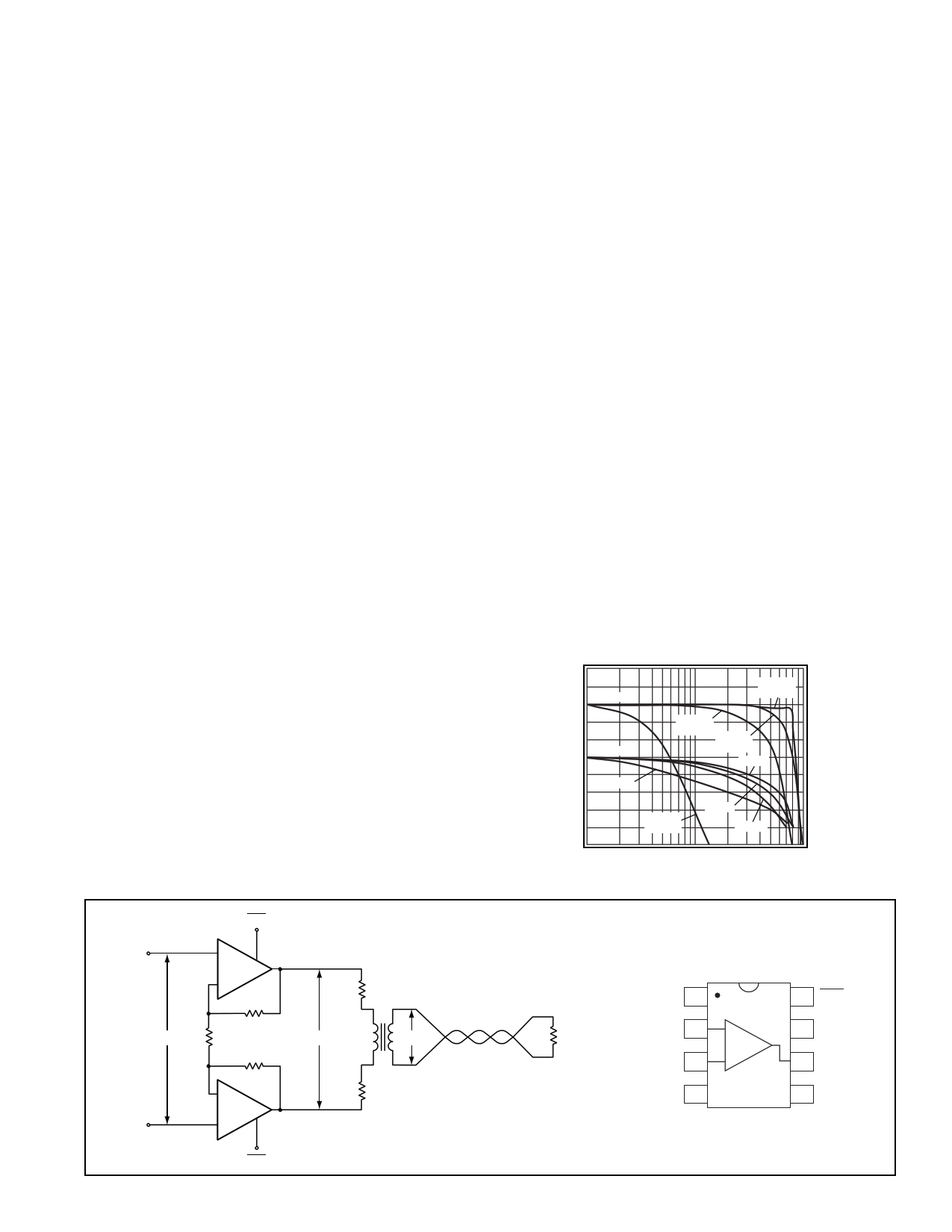
Differential Line Driver With Load
Impedance Conversion
The circuit shown in Figure 7, operates as a differential
line driver. The transformer converts the load impedance
to a value that best matches the CLC5665’s output
capabilities. The single-ended input signal is converted
to a differential signal by the CLC5665. The line’s
characteristic impedance is matched at both the input
and the output. The schematic shows Unshielded Twisted
Pair for the transmission line; other types of lines can also
be driven.
Rg2
Vin
Rt1
Vd/2
+
CLC5665
-
Rf1
Rg1 Rt2
Rf2
- -Vd/2
CLC5665
+
Rm/2
Req
1:n
Rm/2
Zo
UTP
Io
RL
+
Vo
-
Figure 7: Differential Line Driver with
Load Impedance Conversion
5 http://www.national.com
5 Page | ||
| Páginas | Total 8 Páginas | |
| PDF Descargar | [ Datasheet CLC5665IMX.PDF ] | |
Hoja de datos destacado
| Número de pieza | Descripción | Fabricantes |
| CLC5665IM | Low Distortion Amplifier with Disable | National Semiconductor |
| CLC5665IMX | Low Distortion Amplifier with Disable | National Semiconductor |
| Número de pieza | Descripción | Fabricantes |
| SLA6805M | High Voltage 3 phase Motor Driver IC. |
Sanken |
| SDC1742 | 12- and 14-Bit Hybrid Synchro / Resolver-to-Digital Converters. |
Analog Devices |
|
DataSheet.es es una pagina web que funciona como un repositorio de manuales o hoja de datos de muchos de los productos más populares, |
| DataSheet.es | 2020 | Privacy Policy | Contacto | Buscar |